Method for manufacturing an optical element to polarize and split incident light

a manufacturing method and optical element technology, applied in the direction of polarizing elements, instruments, photomechanical devices, etc., can solve the problems of inability to improve the transmission rate or contrast (extinction ratio) of the polarizing element in full measure, and the inability to apply a low viscosity resist made for nano-fabrication in a thin and uniform layer onto such concave-convex face. achieve the effect of improving the optical performance and improving the optical performance of the optical elemen

Active Publication Date: 2012-08-21
SEIKO EPSON CORP
View PDF6 Cites 10 Cited by
  • Summary
  • Abstract
  • Description
  • Claims
  • Application Information

AI Technical Summary

Benefits of technology

[0011]An advantage of the present invention is to provide a method for manufacturing an optical element with which uniform fine lines can be provided on a diffractive structure of a substrate and it is possible to improve optical performance. Another advantage of the invention is to provide an optical element thereof.
[0012]According to one aspect of the invention, a method for manufacturing an optical element that has a function to polarize and split incident light includes: a) forming a grid portion on a face of a substrate in a plural number with a predetermined pitch, b) forming a diffractive structure resist pattern on the face of the substrate, the diffractive structure resist pattern corresponding to a diffractive structure that has a plurality of concave portions and a plurality of convex portions, the concave portions and the convex portions being arranged alternatively on the face of the substrate, c) forming the diffractive structure by etching the substrate anisotropically in a thickness direction with the diffractive structure resist pattern, and d) forming a fine line on the grid portion by depositing a reflective material from an oblique direction onto the face of the substrate where the diffractive structure is provided, the fine line being provided in a direction in which the grid portion extends.
[0013]According to the method, the grid portion can be formed while the face of the substrate is flat so that the width of the grid portion in the shorter direction becomes uniform. In the face of the substrate on which the grid portions having the uniform width, a part which is not covered with the resist is anisotropically etched in the thickness direction of the substrate. After the etching, the part exposed from the resist turns into the concave portion of the diffractive structure, while the width of the grid portion in the shorter direction remains unchanged. At the same time, the part covered with the resist turns into the convex portion of the diffractive structure. In this way, it is possible to equalize the width of the grid portion that is provided in the concave portion to the width of the grid portion that is provided in the convex portion, both the width is measured in the shorter direction of the grid portion. In other words, it is possible to form the grid portion whose width in the shorter direction is uniform in the concave portion and the convex portion of the diffractive structure. Consequently it is possible to improve the optical performance of the optical element.
[0014]It is preferable that the step a) include e) forming a grid portion resist pattern that corresponds to the grid portion on the face of the substrate by a photolithography method, and f) etching the substrate anisotropically in the thickness direction with the grid portion resist pattern.
[0015]In this way, the grid portion resist pattern can be formed while the face of the substrate is flat. Thereby it is possible to make the exposure condition of the grid portion resist pattern uniform. Consequently it is possible to form a resist pattern having a stripe shape that corresponds to the pattern of the grid portion and whose lines are uniform in width in the shorter direction.
[0016]It is also preferable that the anisotropic etching processes performed in the step c) and the step f) be a dry-etching process that uses the same etching gas.

Problems solved by technology

The diffractive structure requires a depth of at least around 100 nm in the concavo-convex face, which makes it almost impossible to apply a low-viscosity resist that is made for nano-fabrication in a thin and uniform layer onto such concavo-convex face.
More specifically, insufficient exposure occurs in the concave portion while excessive exposure occurs in the convex portion, accordingly a width of the resist in a shorter direction becomes large at the concave portion and a width of the resist in a shorter direction becomes small at the convex portion.
As a result, widths of the fine metal lines in the shorter direction are made not uniform since they are fabricated by etching that uses the above-described resist.
With such fine metal lines, it is impossible to improve a transmission rate or contrast (an extinction ratio) of the polarizing element in full measure.
However it is difficult to align and imprint a resist pattern that reaches the bottom for an appropriate etching onto the concavo-convex face, and it significantly impairs efficiency in terms of mass production and the like.

Method used


Image

  • Method for manufacturing an optical element to polarize and split incident light
  • Method for manufacturing an optical element to polarize and split incident light
  • Method for manufacturing an optical element to polarize and split incident light

Examples


Embodiment Construction

[0031]Embodiments of the invention will be described. In the drawings which will be referred in the following description, a scale size may be different in each member or layer in order to make each member or layer recognizable.

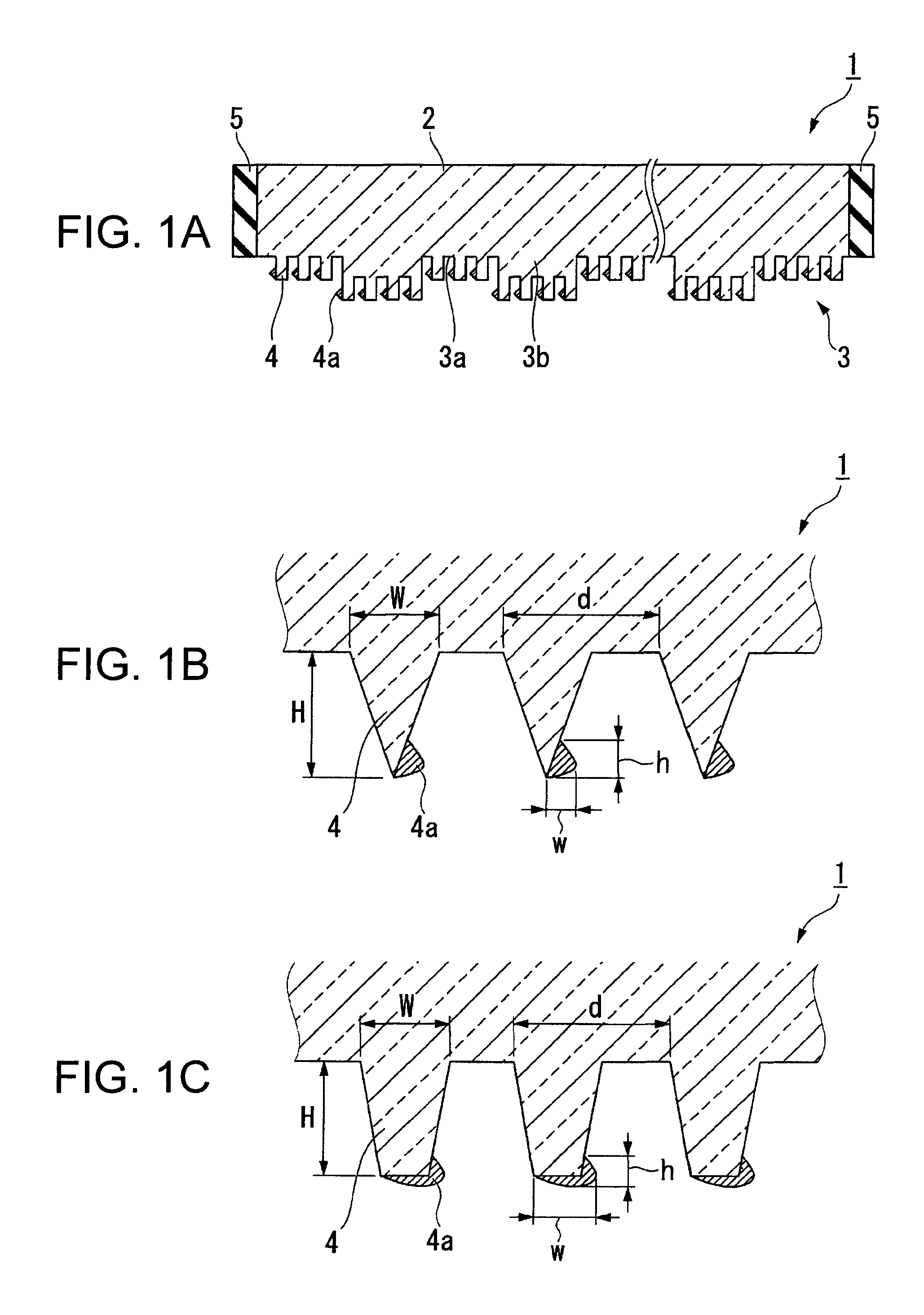
[0032]FIG. 1A schematically illustrates a sectional structure of an optical element according to an embodiment of the invention. FIGS. 1B and 1C are enlarged views of FIG. 1A.

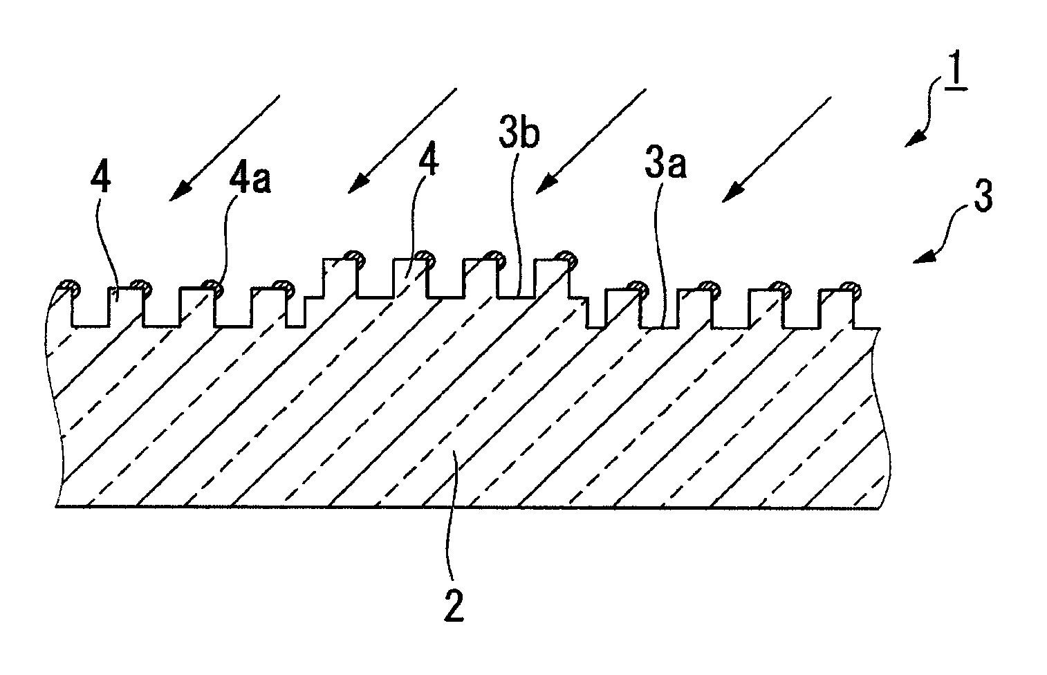
[0033]Referring to FIG. 1A, an optical element 1 according to the embodiment includes a substrate 2, a diffractive structure 3, a grid portion 4 and a light absorber 5. The optical element 1 has a function to polarize and separate incident light with the grid portion 4.

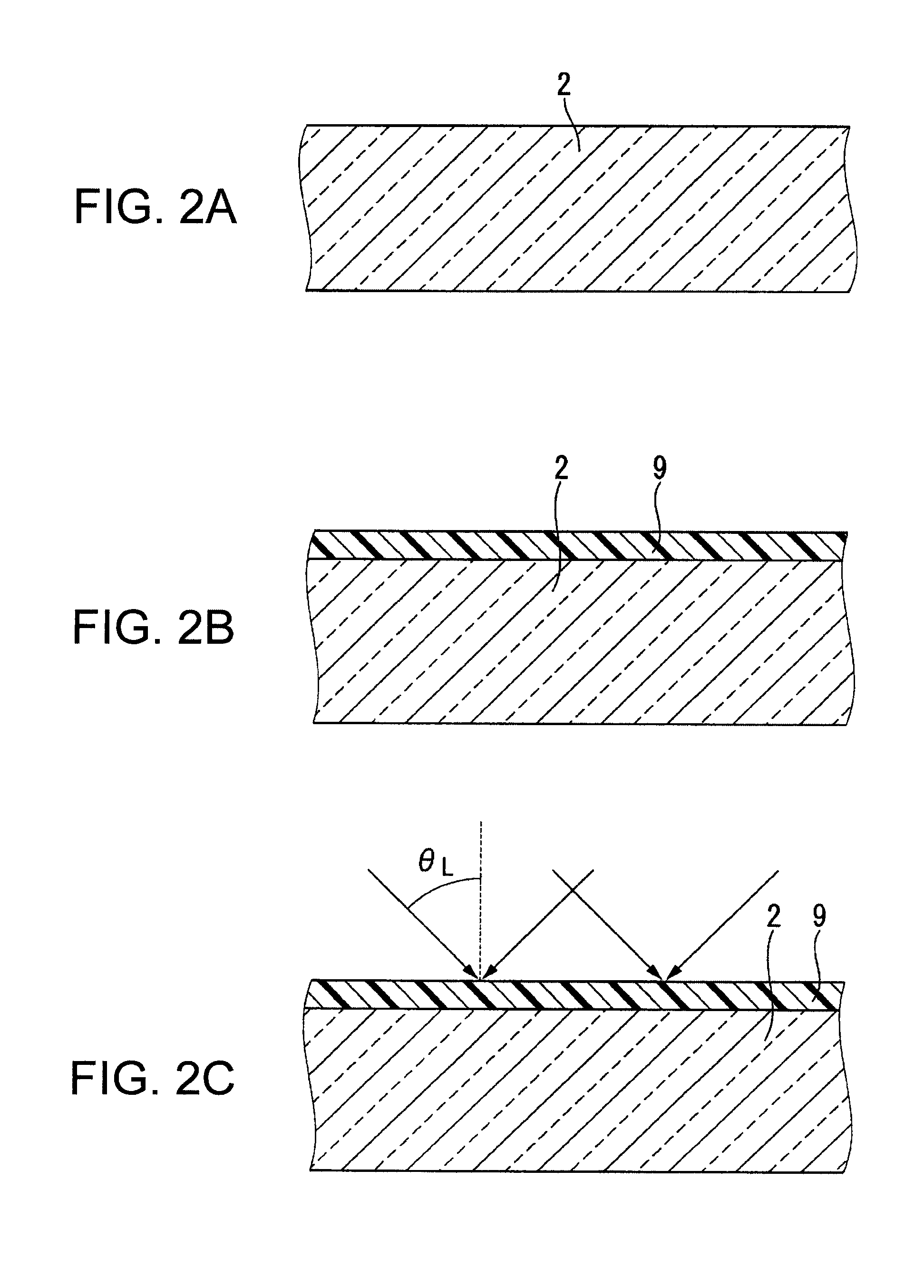
[0034]The substrate 2 is transparent to wavelength of the incident light. For the substrate 2, a substrate made of an inorganic material such as a glass (quartz) substrate can be adopted. A thickness of the substrate 2 is for example about 0.7 mm. On one side of the substrate 2, the diffractive structure 3 is provided. The...


PUM


Abstract

A method for manufacturing an optical element that has a function to polarize and split incident light includes: a) forming a grid portion on a face of a substrate in a plural number with a predetermined pitch; b) forming a diffractive structure resist pattern on the face of the substrate; c) forming the diffractive structure by etching the substrate anisotropically in a thickness direction with the diffractive structure resist pattern; and d) forming a fine line on the grid portion by depositing a reflective material from an oblique direction onto the face of the substrate where the diffractive structure is provided.

Description

CROSS-REFERENCE TO RELATED APPLICATION[0001]This application is based on and claims priority from Japanese Patent Application No. 2009-009619, filed on Jan. 20, 2009, the contents of which are incorporated herein by reference.BACKGROUND[0002]1. Technical Field[0003]The present invention relates to a method for manufacturing an optical element that has a polarizing beam-splitting function. The invention also relates to an optical element.[0004]2. Related Art[0005]Among optical elements having a polarizing beam-splitting function, there is known a polarizing beam-splitting element of a wire grid type. JPA-2006-133275 is an example of related art. The wire grid type polarizing beam-splitting element is manufactured for example through the following steps. A concavo-convex structure, which serves as a diffractive structure, is firstly formed on a light transmissive substrate by using a photolithography method, an etching method or the like. Subsequently an aluminum film that covers a su...

Claims


Application Information

Patent Timeline
Patent Type & Authority Patents(United States)
IPC IPC(8): G02B5/30
CPCG02B5/1861G02B5/3058B29D11/00634G02B5/1857
Inventor KENMOCHI, NOBUHIKO
Owner SEIKO EPSON CORP
Why Eureka
Try Eureka