Method for improved patterning accuracy for thin film photovoltaic panels

a thin film photovoltaic panel and patterning technology, applied in the direction of liquid surface applicators, coatings, semiconductor devices, etc., can solve the problems of reducing the efficiency of cell efficiency, and reducing the cost of petrochemical fuel supply, etc., to achieve the effect of improving the cell-spacing accuracy, simplifying the patterning of the thin film panel after the thermal process, and improving cell efficiency

Inactive Publication Date: 2012-09-11
CM MFG
View PDF231 Cites 21 Cited by
  • Summary
  • Abstract
  • Description
  • Claims
  • Application Information

AI Technical Summary

Benefits of technology

[0009]Many benefits can be achieved by applying the embodiments of the present invention. Particularly, the method provides a method for patterning a thin film photovoltaic panel device with improved cell-spacing accuracy. By taking account a physical compaction of the substrate due to a predetermined thermal process, patterning of the thin film on the substrate before the thermal process can be transformed in a controlled fashion after going through the thermal process. Patterning of the thin film panel after the thermal process then can then be simplified using a mechanical scriber with multiple fixed tips. Each tip can be pivoted and applied a desired force to scribe a predetermined depth through a window layer and / or the absorber layer of the photovoltaic film stack for patterning each of a plurality of photovoltaic cells on the substrate. Preferably, the first series of patterns are performed using laser scribing with predetermined positioning to make proportional expanded inter-pattern spacing based on a compaction parameter of the substrate. The proportional expansion of the inter-pattern spacing then is substantially compensated following the thermal process for absorber layer to provide uniformly spaced patterns. In an embodiment, the second (or more) series of patterns can be, formed by mechanical scribing, for example, four or more equally spaced pivoted tips. The patterning process performed according to embodiments of the invention results in a well defined electrical connection structure for each photovoltaic cell substantially without wasting the spatial region between patterns for non photovoltaic function, thus greatly enhancing the cell efficiency.

Problems solved by technology

Unfortunately, the supply of petrochemical fuel is limited and essentially fixed based upon the amount available on the planet Earth.
Additionally, as more people use petroleum products in growing amounts, it is rapidly becoming a scarce resource, which will eventually become depleted over time.
Although solar energy is environmentally clean and has been successful to a point, many limitations remain to be resolved before it becomes widely used throughout the world.
However, crystalline materials are often costly and difficult to make on a large scale.
Similar limitations exist with the use of thin film technology in making solar cells.
That is, efficiencies are often poor.
Additionally, film reliability is often poor and cannot be used for extensive periods of time in conventional environmental applications.
Often, thin films are difficult to mechanically integrate with each other.

Method used


Image

  • Method for improved patterning accuracy for thin film photovoltaic panels
  • Method for improved patterning accuracy for thin film photovoltaic panels
  • Method for improved patterning accuracy for thin film photovoltaic panels

Examples


Embodiment Construction

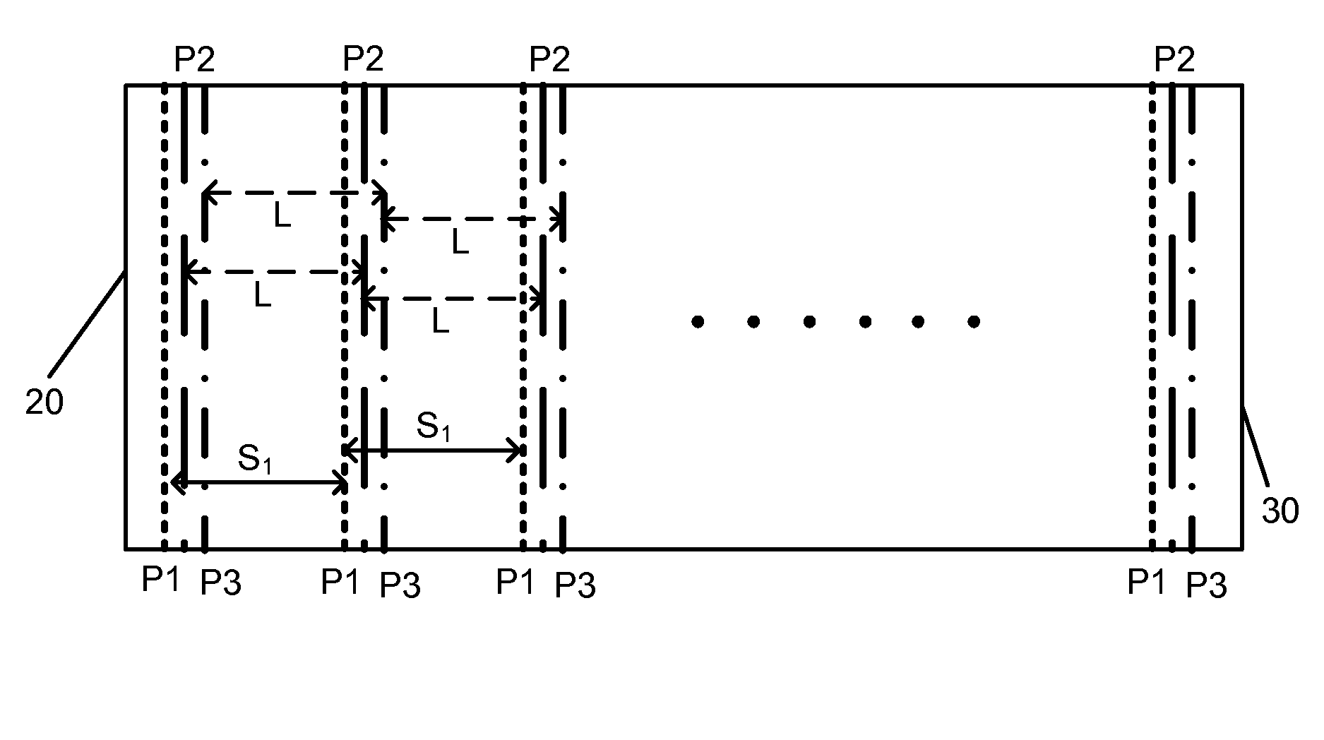
[0014]Embodiments according to the present invention relates to photovoltaic materials and manufacturing method. More particularly, the present invention provides a method and structure for patterning thin film photovoltaic panels with improved accuracy. Merely by way of example, the present method and structure include forming a first series of patterns with pre-compensated inter-pattern spacing followed by a second series of patterns after substrate compaction in thermal processing. The method is applied to a thin-film stack for manufacturing copper indium diselenide based thin film photovoltaic devices, but it would be recognized that the invention may have other configurations.

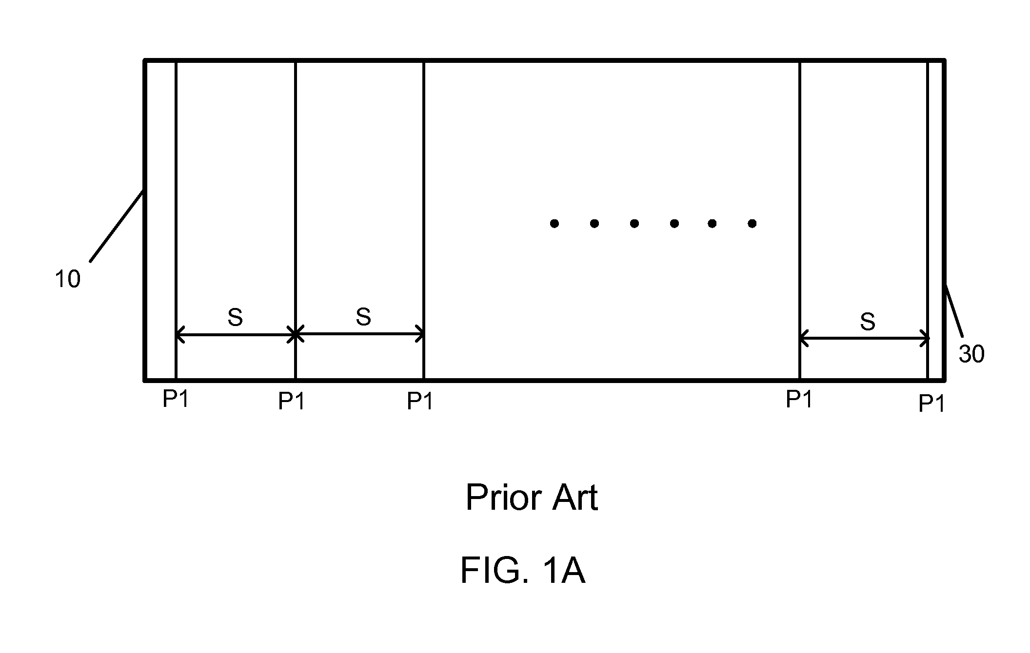
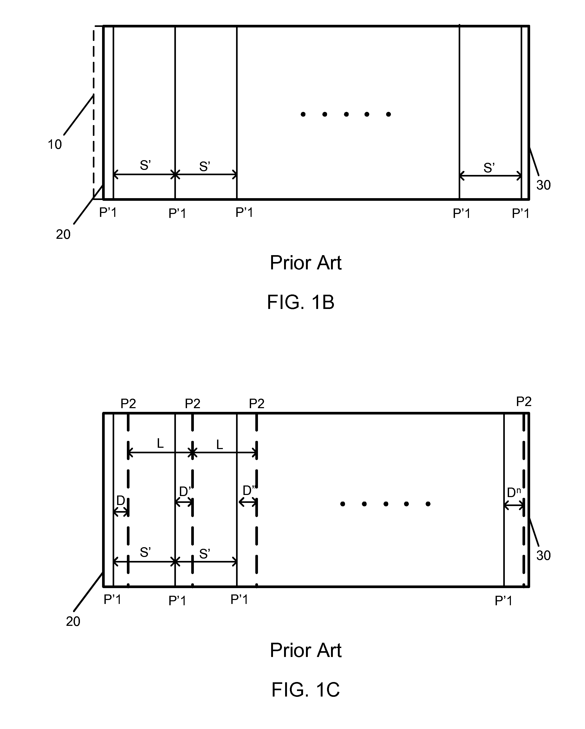
[0015]The state of art manufacturing process of thin film based photovoltaic cell requires multiple stages of patterning process to scribe line patterns for a plurality of cells formed on a large substrate panel. Each cell usually is designed to cover a same spatial area of the panel so that patterning can...


PUM

PropertyMeasurementUnit
temperatureaaaaaaaaaa
glass strain pointaaaaaaaaaa
radiusaaaaaaaaaa

Abstract

A method for patterning a thin film photovoltaic panel on a substrate characterized by a compaction parameter. The method includes forming molybdenum material overlying the substrate and forming a first plurality of patterns in the molybdenum material to configure a first patterned structure having a first inter-pattern spacing. Additionally, the method includes forming a precursor material comprising at least copper bearing species and indium bearing species overlying the first patterned structure. Then the substrate including the precursor material is subjected to a thermal processes to form at least an absorber structure.

Description

CROSS-REFERENCE TO RELATED APPLICATION[0001]This application claims priority to U.S. Provisional Patent Application No. 61 / 298,185, filed Jan. 25, 2010, entitled “Method for Improved Patterning Accuracy for Thin Film Photovoltaic Panels” by inventor Frank Patterson, commonly assigned and incorporated by reference herein for all purposes.BACKGROUND OF THE INVENTION[0002]The present invention relates generally to photovoltaic materials and manufacturing method. More particularly, the present invention provides a method and structure for patterning thin film photovoltaic panels with improved accuracy. Merely by way of example, the present method and structure include forming a first series of patterns with pre-compensated inter-pattern spacing followed by additional series of patterns after substrate compaction in thermal processing. The method is applied to a thin-film stack for manufacturing copper indium diselenide based thin film photovoltaic devices, but it would be recognized tha...

Claims


Application Information

Patent Timeline
Patent Type & Authority Patents(United States)
IPC IPC(8): H01L21/44
CPCH01L31/0322H01L31/0463Y02E10/541
Inventor PATTERSON, FRANK
Owner CM MFG
Why Eureka
Try Eureka