
Nonvolatile optical memory element, memory device, and reading method thereof

a memory element and non-volatile technology, applied in the direction of information storage, static storage, digital storage, etc., can solve the problems of limiting the speed of data processing by opto-electronic conversion, the operation speed of these devices is the electron intersubband lifetime, and the operation speed of these devices is rather long in a semiconductor, so as to achieve a widening a significant expansion of the effective magneto-optical region

Inactive Publication Date: 2012-09-18
NAT INST OF ADVANCED IND SCI & TECH
View PDF10 Cites 0 Cited by
  • Summary
  • Abstract
  • Description
  • Claims
  • Application Information

AI Technical Summary

Benefits of technology

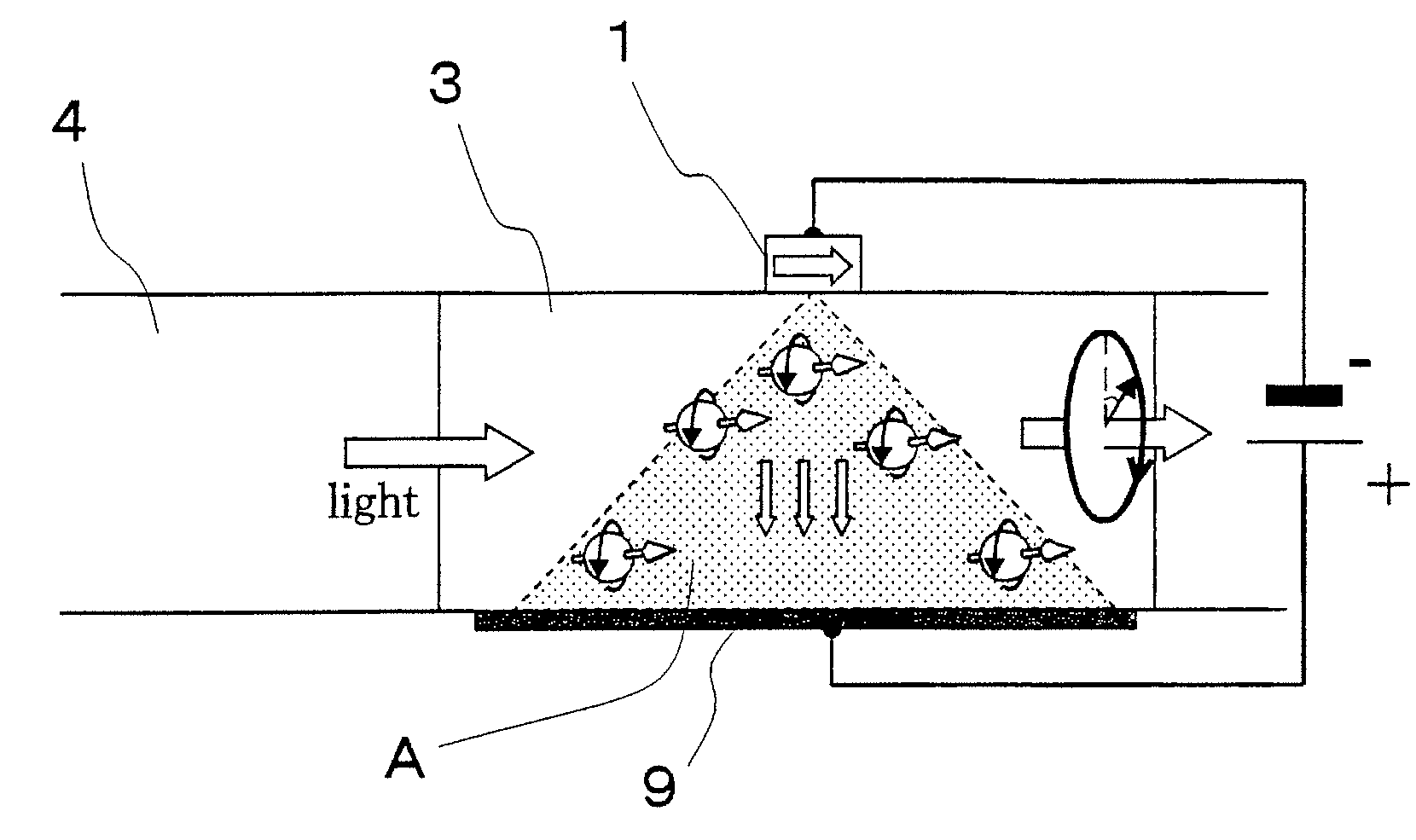
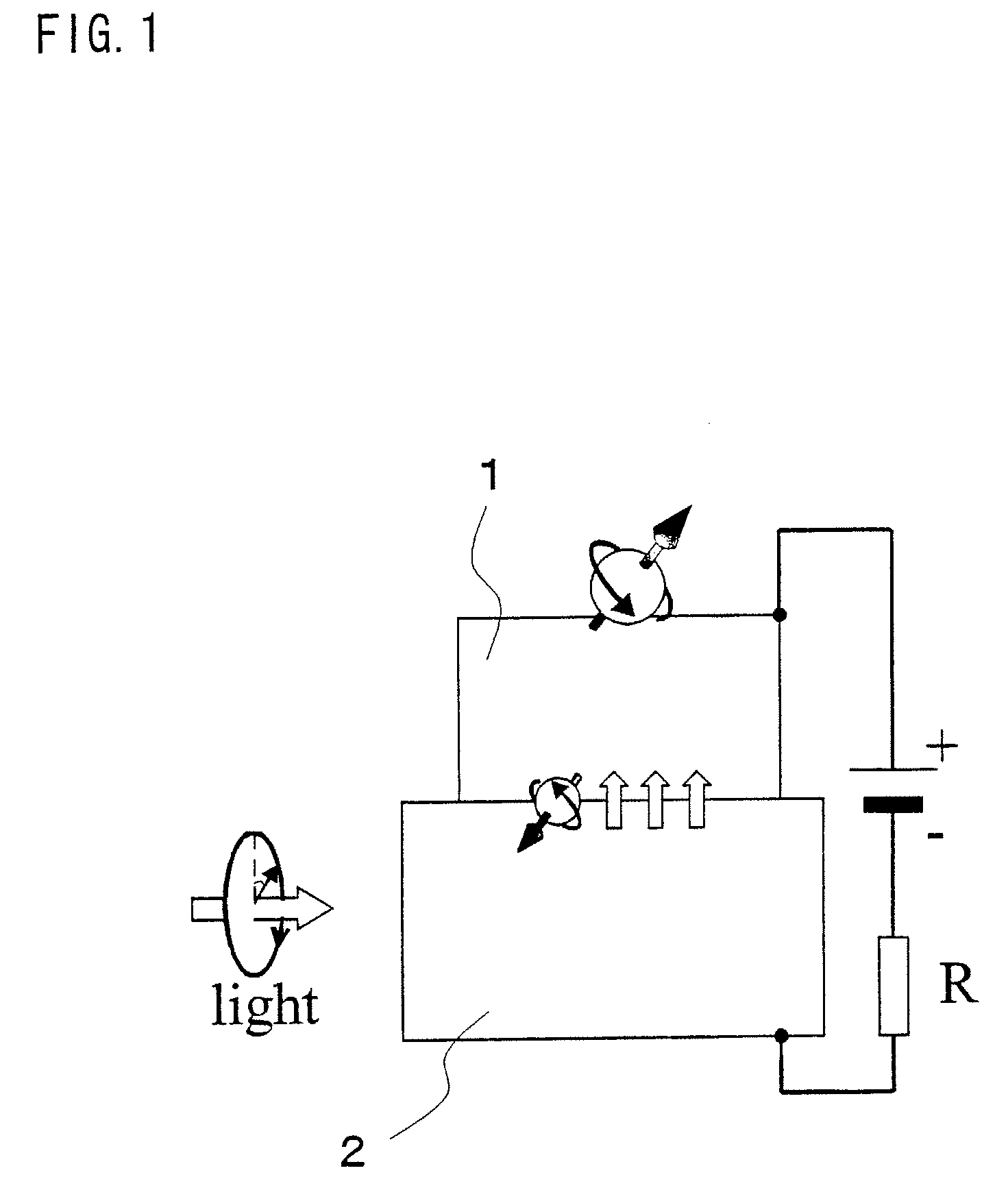
[0037]In the memory element of the present invention, light passing through a semiconductor region experiences the magneto-optical effect due to the injection of spin-polarized electrons into a semiconductor from a nanomagnet, which is a micro-sized ferromagnetic body in a single-magnetic structure (single domain). In addition, the effective magneto-optical region broadens due to the wide spreading of spin-polarized electrons in the semiconductor region. This yields an effect that a significant magneto-optical signal is generated. As a result, the effective magneto-optical region can be significantly enlarged comparing to conventional techniques. In the conventional techniques of reading a magneto-optical signal, it was impossible to detect an output from a nanomagnet having a size of 200 nm×200 nm or less. In contrast, with the use of the memory element of the present invention, by performing the spin injection from a nanomagnet into a semiconductor by applying an electrical pulse, the output of the magneto-optical signal can be increased, thereby allowing data reading. Moreover, a bigger magneto-optical signal can be obtained by enlarging an amplification region in the semiconductor. Further, the memory device of the present invention is arranged such that: a plurality of the memory elements of the present invention is provided, and optical waveguides connect the memory elements to an optical pulse source; optical path lengths of the optical waveguides are adjusted so that an optical pulse passes through the memory elements so that the memory elements outputs respective optical pulses having different delays; and the respective optical pulses are combined at an output side of the memory device. This allows high-speed data reading from the memory device of the present invention by means of a consecutive optical pulse train. Further, in the memory device of the present invention, an electrical pulse and an optical pulse are applied to the memory elements so that a magnetization direction of a nano-sized memory element can be read as intensity of the optical pulse train due to the magneto-optical effect. This allows higher-speed data reading with a high SN ratio.

Problems solved by technology

The opto-electronic conversion limits the speed of data processing.
Major limitation for the fast operational speed of these devices is the electron intersubband lifetime, which is rather long in a semiconductor.
Also, those memories are volatile; therefore they can store data only for rather short time interval.

Method used


Image

  • Nonvolatile optical memory element, memory device, and reading method thereof
  • Nonvolatile optical memory element, memory device, and reading method thereof
  • Nonvolatile optical memory element, memory device, and reading method thereof

Examples


example 1

[0076]FIG. 7 shows a structural example of the nonvolatile optical memory element used in the first and second embodiments. A spin-photon memory in Example 1 includes a substrate 46, an optical waveguide buffer layer 45, a waveguide core layer 44, a p-i-n semiconductor detector 43, which functions as a semiconductor optical amplifier, a buffer layer 42, and a nanomagnet 41. These members are stacked in this order. The substrate 46 is made of a p-type GaAs 38, and on one side of the substrate 46 is disposed a Cr / Au electrode 39. On another side of the substrate 46 which is opposite to the side of the substrate 46 on which the electrode 39 is disposed, the optical waveguide buffer layer 45 made of a p-type Al0.5Ga0.5As 37 and the optical waveguide core layer 44 made of a p-type Al0.3Ga0.7As 36 are provided. The p-i-n semiconductor detector 43, which functions as a semiconductor optical amplifier, is constituted by a p-type GaAs 35, an i-type GaAs 34, and an n-type GaAs 33. The nanomag...

example 2

[0078]Example 2 is a structural example in which a photodetector, which functions as an optical amplifier, is disposed on an optical waveguide. FIG. 8 shows the structure. An optical waveguide structure is constituted by a p-type GaAs 58, a p-type Al0.5Ga0.5As 57, and a p-type Al0.3Ga0.7As optical waveguide core 56. On one side of the optical waveguide structure is provided an electrode 59 made of Cr / Au. On another side of the optical waveguide structure are provided a p-type GaAs 55, an i-type GaAs 54, and an n-type GaAs 53, which are sequentially provided on the optical waveguide core, so as to constitute a p-i-n semiconductor detector, which functions as an optical amplifier. A buffer layer made of an nn-type GaAs 52 is provided on a top of the p-i-n semiconductor detector, and a Fe layer 51 is provided on a top of the nn-type GaAs 52. A voltage source is connected between the Fe layer 51, which serves as a nanomagnet, and the electrode 59. As shown in FIG. 8, when light is incid...

example 3

[0081]Example 3 is a structural example of an optical waveguide into which a photodetector, which functions as an optical amplifier, is embedded. FIG. 9 shows the structure. An optical waveguide structure is constituted by a p-type GaAs 68, a p-type Al0.5Ga0.5As 67, and an i-type Al0.3Ga0.7As optical waveguide core 66. On one side of the optical waveguide structure is provided an electrode 69 made of Cr / Au. On another side of the optical waveguide structure, a groove is formed from a top surface of the optical waveguide core so that a p-type GaAs 65, an i-type GaAs 64, and an n-type GaAs 63 are sequentially provided in the groove, so as to constitute a p-i-n semiconductor detector, which functions as an optical amplifier. A buffer layer made of an nn-type GaAs 62 is provided on a top of the p-i-n semiconductor detector, and a Fe layer 61 is provided on a top of the nn-type GaAs 62. A voltage source is connected between the Fe layer 61, which serves as a nanomagnet, and the electrode...


PUM


Abstract

A nonvolatile optical memory element in which a ferromagnetic body is provided on a semiconductor causes such a problem that in a case where magnetization of the ferromagnetic body is read by light, magneto-optical response becomes very small when the ferromagnetic body is small in volume. The present invention provides a memory element, a memory device, and a data reading method, each of which is applicable to data reading from a nonvolatile optical memory element. In a nonvolatile optical memory element having a structure in which a ferromagnetic body is provided on a semiconductor that is connected to an optical waveguide, electrons are injected into the semiconductor via the ferromagnetic body so that the electrons that are spin-polarized according to a magnetization direction of the ferromagnetic body are injected into the semiconductor, thereby enlarging a region in which a photomagnetic effect occurs effectively. By applying an electric pulse and an optical pulse to the nonvolatile optical memory element, it is possible to effectively read recorded data according to a magnetization direction of the ferromagnetic body.

Description

[0001]This Nonprovisional application claims priority under 35 U.S.C. §119(a) to Patent Application No. 2009-177145 filed in Japan on Jul. 30, 2009, the entire contents of which are hereby incorporated by reference.TECHNICAL FIELD[0002]This invention relates to a nonvolatile optical memory element, such as a spin-photon memory that uses spin injection, a method for reading data from the nonvolatile optical memory element, a memory device including the nonvolatile optical memory elements, and a method for reading data from the memory device.Background Art[0003]A high-speed nonvolatile optical memory is very important for optical networks. High-speed data processing such as a receiving, a storing and a resending of data are the main functions of an optical network server. At present, a buffer memory made of electronic components in combination with an opto-electronic converter is employed for these functions. The opto-electronic conversion limits the speed of data processing. For fast...

Claims


Application Information

Patent Timeline
Patent Type & Authority Patents(United States)
IPC IPC(8): G11C13/06
CPCG11C13/06
Inventor ZAYETS, VADYMANDO, KOJIYUASA, SHINJISAITO, HIDEKAZU
Owner NAT INST OF ADVANCED IND SCI & TECH
Learn More