
Rectilinear covering method with bounded number of rectangles for designing a VLSI chip

a technology of vlsi chips and rectangles, applied in the direction of instruments, computing, electric digital data processing, etc., can solve the problems of increasing the time-to-market introduction, increasing the cost of manufacturing, and the current design tools are presently reaching the limit of efficiency and speed, so as to reduce the area of metal layers, reduce the cost of manufacturing, and reduce the effect of total real esta

Inactive Publication Date: 2012-10-23
IBM CORP
View PDF8 Cites 5 Cited by
  • Summary
  • Abstract
  • Description
  • Claims
  • Application Information

AI Technical Summary

Benefits of technology

[0035]In one aspect of the invention, routing a VLSI design layout includes minimizing the area of the metal layer, minimizing the total real estate. The number of bounded rectangles increases the manufacturability through Design for Manufacturability (DFM) and Optical Proximity Correction (OPC) and reduces the number of corners to improve the OPC.
[0038]In yet another aspect of the present invention, the netlist for a given set of input terminals is represented by a set of input points, wherein the ensuing a rectilinear polygon is simple for further processing, e.g., by Optical Proximity Correction (OPC). The present invention also creates a tight bound for a group of pixilated source generated by a Source Mask Optimization (SMO) method, in which case, the output source pixels can be advantageously used as a set of input points, and having the tightly bound group of pixels forming a rectilinear polygonal source. The present invention further creates a tight bound for a group of errors generated by an ORC or Design Rules Checking method, using the output error locations as input points, the tight bound for the group of errors forming the rectilinear polygon.

Problems solved by technology

Design automation of complex VLSI chips is often associated to a lengthy design turnaround time which, in turn, increases the time-to-market introduction.
Two reasons for the large turnaround time problem include: slowness of the algorithms caused by large problem sizes (e.g., hundreds of millions of circuits and nets on a chip), and the large number of iterations between different algorithms requiring convergence to an acceptable level.
Current design tools are presently reaching the limit of their efficiency and speed as the number of circuit components such as transistors, diodes, capacitors, resistors, and the like, increase exponentially, and the complexity of their connectivity increases geometrically in term of the number of components.
A major critical issue for any type of partitioning in the development of VLSI design automation algorithm is directed to the chip real estate.
Normally, there exists an upper bound on the number of such partitions that can be used to solve a particular problem since, as the number of partitions increases, the complexity of the algorithm(s) increases with it.
However, the ever shrinking device dimensions combined with the desire to enhance circuit performance in the deep sub-wavelength domain require complex OPC methodologies to ensure the fidelity of mask patterns of the printed wafer.
While the quality of the OPC may improve as the number of segments increases, the efficiency of the MBOPC tool may decrease as the number of segments it simulates and iterates over in each iterative step increases.
In case of destructive interferences, the light beams weaken each other and weaken the total effect of the light.
The object of SMO resides in determining the light pixels requiring to be turned on, such that the constructive interferences strengthen the effect of light where there is a need to have light on the wafer, and destructive interferences weaken the effect of light where no light is to be present thereon.
Notwithstanding the above, it is still difficult and costly to construct a pixilated source as illustrated by, e.g. 301 and 310 (FIG. 3).
The ever increasing cost of mask manufacturing and inspection and the ever increasing complexity of OPC and RET requires that the mask be correctly and accurately simulated for potential defects before the mask is manufactured.
The cost of finding an error when the mask is actually manufactured and used for chip manufacturing is very high.
Since a missed error is significantly more expensive than a false error, all the ORC tools are expected to err on the conservative side.
If there are too many, the real errors may be missed by the manual inspection, requiring a significant amount of time to shift through all the false errors to find the real errors.
Current ORC methods tend to simulate the entire mask layout image with the most accurate geometry using conservative criteria and, further, and which have a tendency of increasing the runtime of the ORC along with the number of false errors.
However, the bounding box does not show a very tight bound.

Method used


Image

  • Rectilinear covering method with bounded number of rectangles for designing a VLSI chip
  • Rectilinear covering method with bounded number of rectangles for designing a VLSI chip
  • Rectilinear covering method with bounded number of rectangles for designing a VLSI chip

Examples


Embodiment Construction

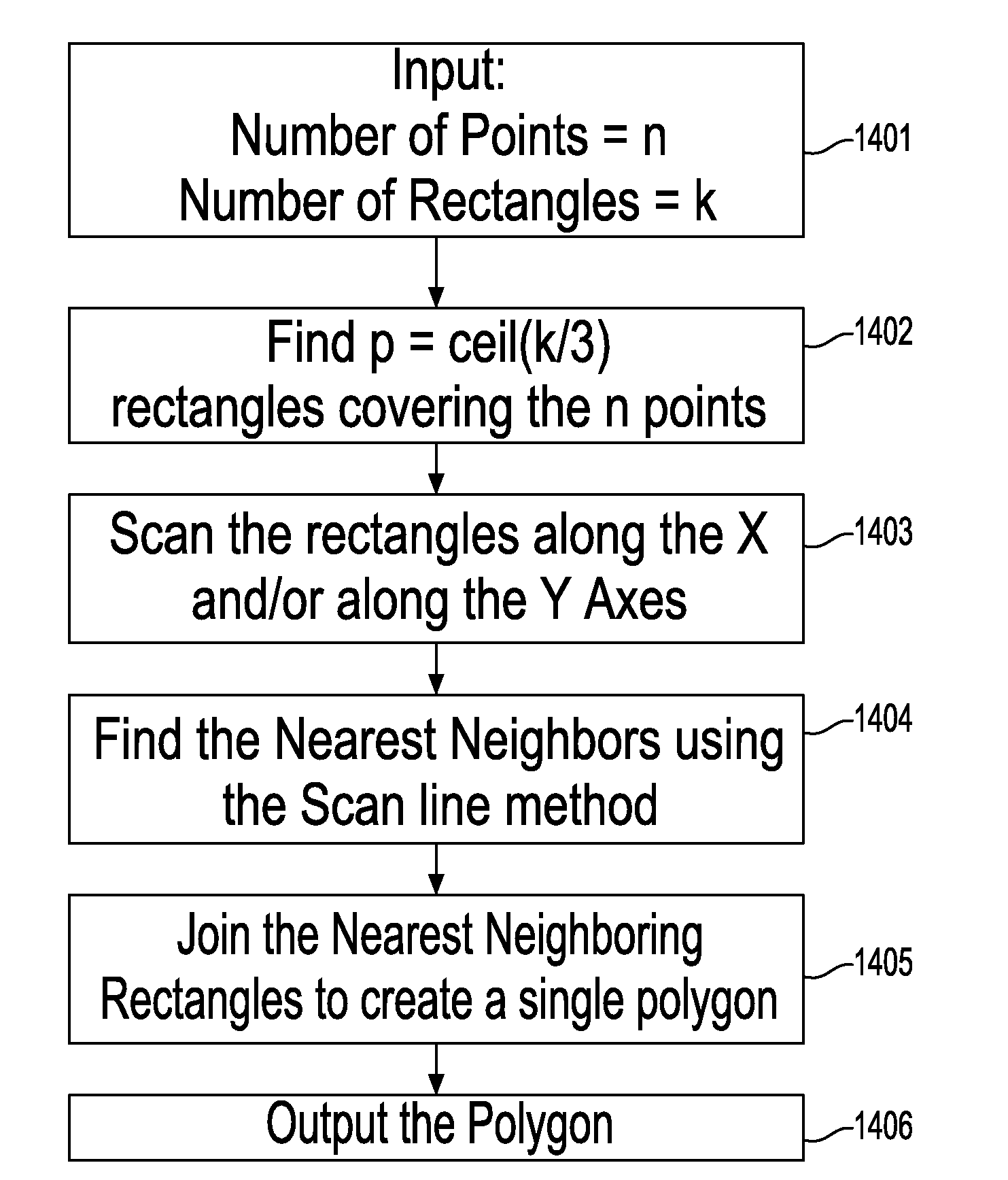
[0064]In describing the preferred embodiment of the present invention, reference will be made in conjunction to FIGS. 5-15, wherein like numerals refer to like features.

[0065]In accordance with one embodiment of the present invention, a flow chart is shown with reference to FIG. 5.

[0066]In step 501, a set of input points n is provided, the number of input points including terminals of the netlist. In another embodiment, the number of input points includes a pixilated source generated by an SMO program. In still another embodiment, the number of input points is shown to include the errors generated by ORC or DRC programs.

[0067]The maximum number of rectangles k is a parameter similar to the one provided in Step 501. The input parameter k defines the ‘simplicity’ of the output rectilinear polygon, wherein the output rectilinear polygon has the smallest area and the rectilinear polygon is covered by the maximum number k of rectangles.

[0068]In the next Step 502, the n input points are f...


PUM


Abstract

A method for creating a rectilinear non-convex polygonal output representative of a component used to build a VLSI circuit chip from a plurality of points corresponding to a plurality of components of the chip includes: covering the plurality of points with a set of rectangles; creating a Voronoi diagram for the set of rectangles; forming a nearest neighbor tree for the Voronoi diagram; connecting a selected set of the rectangles corresponding to the nearest neighbor tree into a non-convex rectilinear polygon; and applying the non-convex rectilinear polygon to build the VLSI chip.

Description

FIELD OF THE INVENTION[0001]The present invention relates to the design and manufacturing of Very Large Scale Integrated chips and, more particularly, to a method of configuring partitions for locating different circuits or other operational areas of the chip.BACKGROUND AND RELATED ART[0002]Very Large Scale Integrated (VLSI) chips include many electronic components (e.g., transistors, resistors, diodes, and the like) interconnected to form multiple circuit components (e.g., gates, cells, memory units, arithmetic units, controllers, decoders, and the like). The electronic and circuit components of the VLSI chip are jointly referred to as “components.”[0003]A conventional VLSI circuit includes multiple layers of wiring (wiring layers) that interconnect the electronic and circuit components. For instance, VLSI chips are fabricated with metal or polysilicon wiring layers (collectively referred hereinafter as metal layers) that interconnect the electronic and circuit components. Common f...

Claims


Application Information

Patent Timeline
Patent Type & Authority Patents(United States)
IPC IPC(8): G06F17/50
CPCG06F17/5068G06F30/39
Inventor MUKHERJEE, MAHARAJ
Owner IBM CORP
Learn More