Defect inspection method and apparatus therefor

a defect inspection and apparatus technology, applied in the field of sample inspection, can solve the problems of low detection sensitivity of defect inspection apparatus, defects with smaller luminance differences than the raised threshold value, and noise during inspection, so as to reduce the influence of luminance variation between compared images arising from the difference in layer thickness or pattern width, high sensitivity, and high speed

Inactive Publication Date: 2012-12-25
HITACHI HIGH-TECH CORP
View PDF10 Cites 10 Cited by
  • Summary
  • Abstract
  • Description
  • Claims
  • Application Information

AI Technical Summary

Benefits of technology

[0008]The invention is thus a defect inspection method and a defect inspection apparatus designed to overcome the above problems associated with conventional defect inspection technologies, in which images of mutually corresponding areas in identically formed patterns on a sample are compared to detect mismatched portions of the images as defects. In accordance with the invention, the influences of luminance variation between compared images arising from the difference in layer thickness or pattern width can be reduced, and only defects of the user's interest can be detected with high sensitivity and at high speed that would otherwise be regarded as noise.

Problems solved by technology

Because such areas, if detected as defects, misinform the user, they are not to be detected as defects.
However, this means at the same time that the inspection sensitivity of the defect inspection apparatus decreases, and defects with smaller luminance differences than the raised threshold value cannot be detected.
In the above conventional inspection based on luminance comparison, such luminance differences may result in noise during inspection.
There are various kinds of defects; accordingly, there are defects that need not be detected (can be regarded as noise) and defects that need be detected.
Although it is demanded of external inspection that only defects of the user's interest be extracted from among a great number of defects, this can hardly be achieved with the above-described comparison between the threshold value and luminance differences.

Method used


Image

  • Defect inspection method and apparatus therefor
  • Defect inspection method and apparatus therefor
  • Defect inspection method and apparatus therefor

Examples


Embodiment Construction

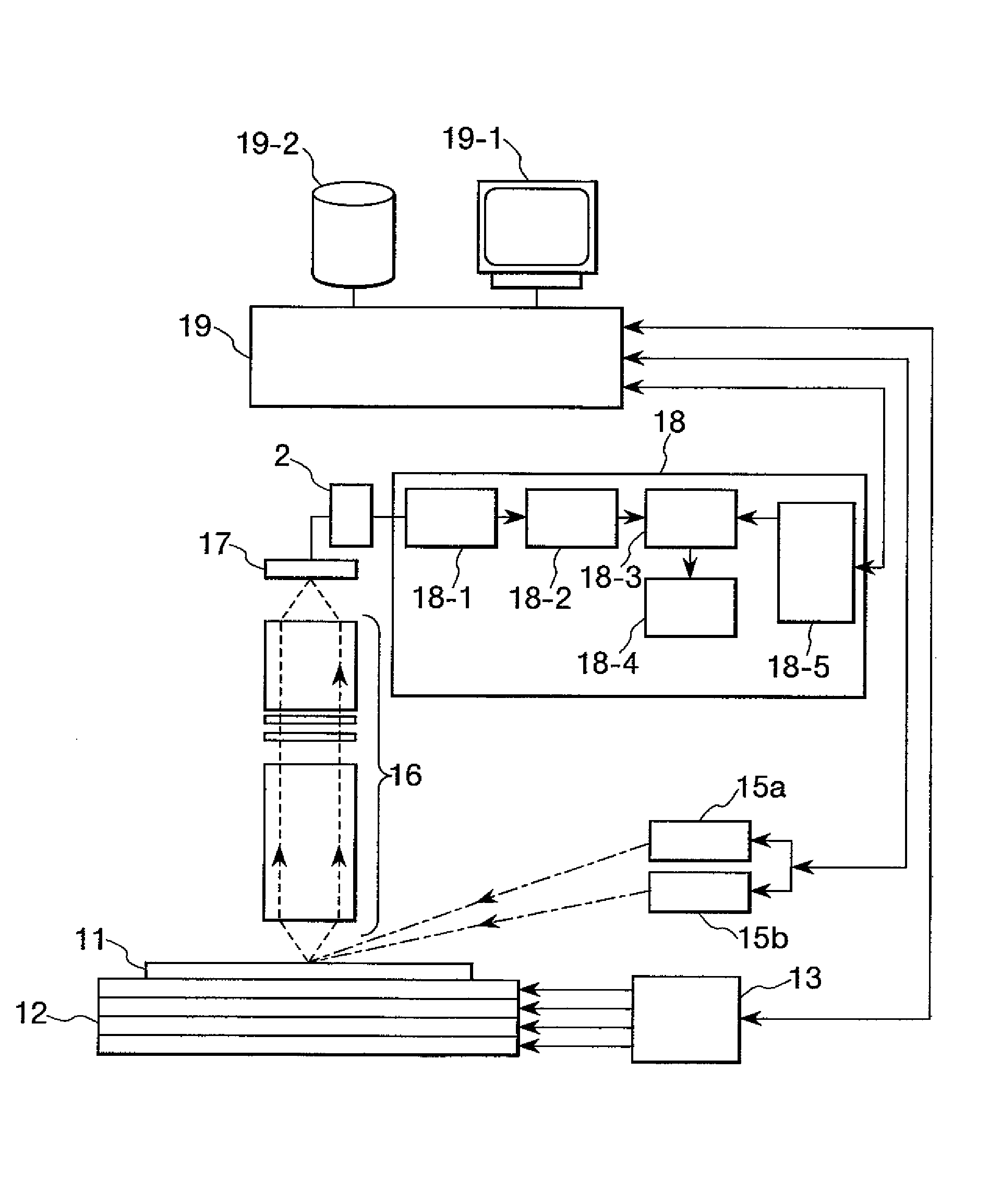
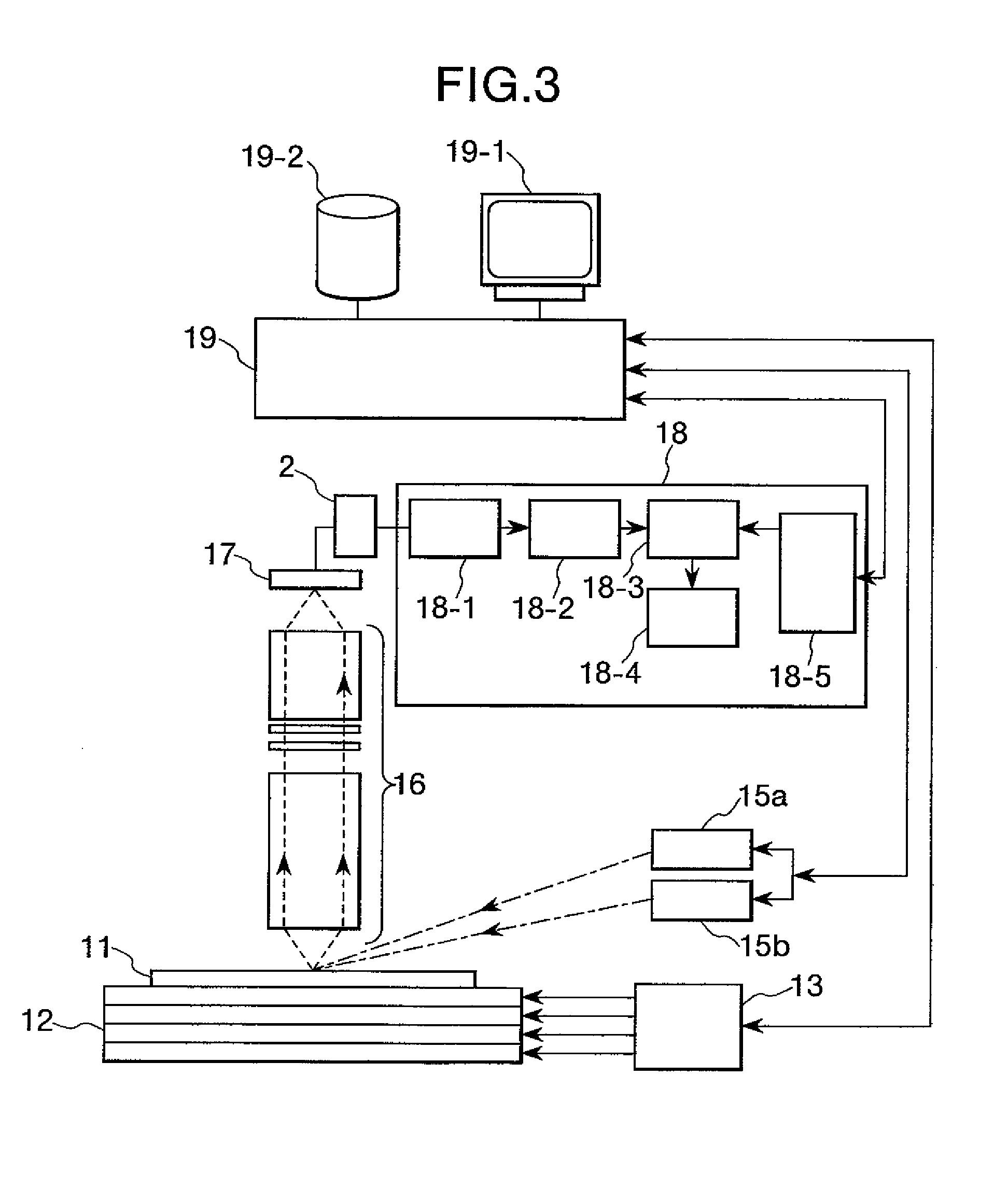
[0054]Preferred embodiments of the present invention are now described with reference to FIGS. 1 to 15. As an example, the defect inspection apparatuses of the embodiments are intended to employ dark-field illumination to inspect semiconductor wafers.

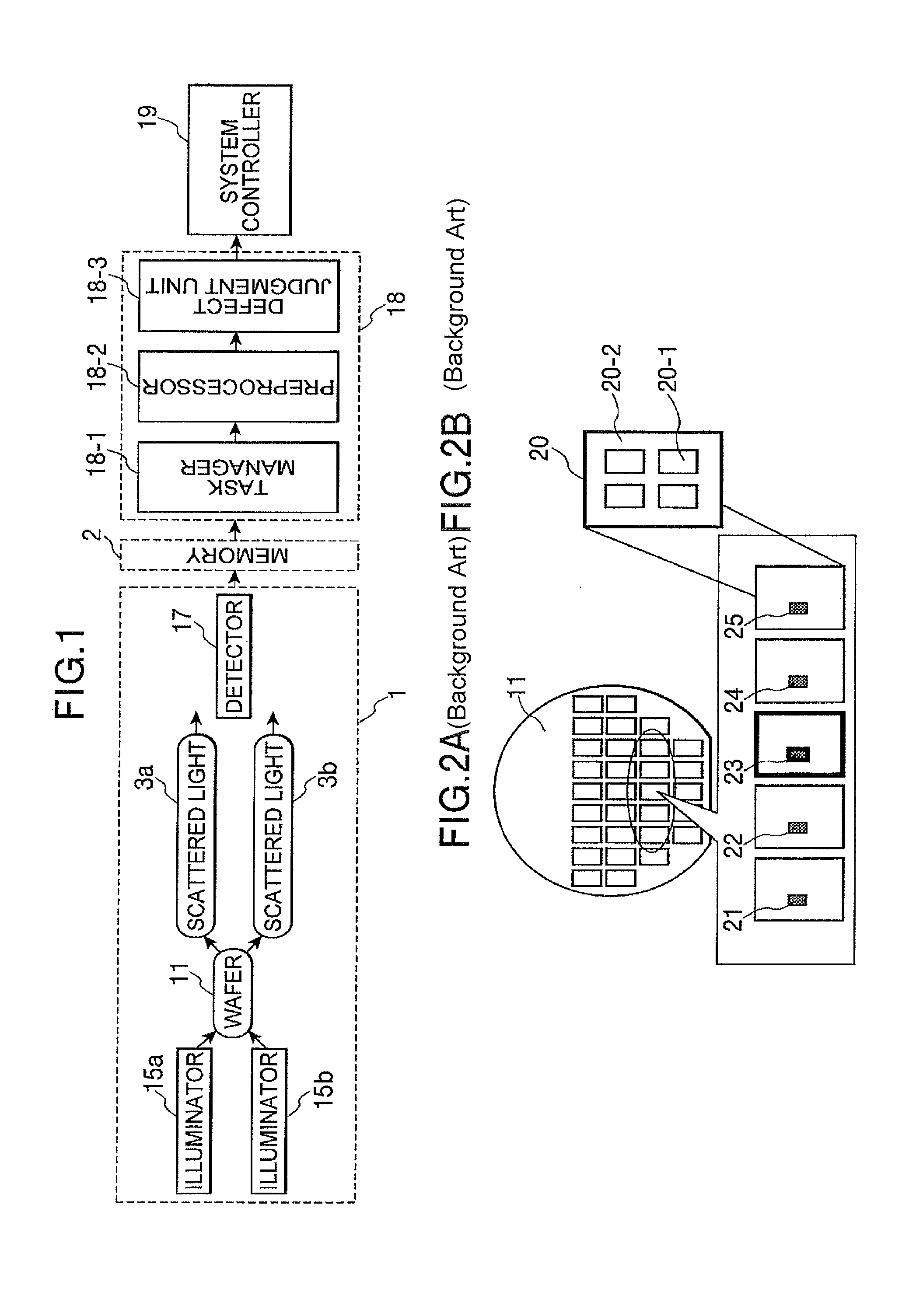
[0055]FIG. 1 is a schematic diagram of a defect inspection apparatus that embodies the invention. As shown in FIG. 1, an optical unit 1 structurally includes multiple illuminators 15a and 15b and a detector 17. The illuminators 15a and 15b emit illumination lights in mutually different optical conditions onto a sample 11 (i.e., a wafer to be inspected). The illumination lights emitted by the illuminators 15a and 15b onto the sample 11 result in scattered lights 3a and 3b, respectively, from the sample 11, which lights are detected as scattered-light intensity signals by the detector 17. Although FIG. 1 illustrates the single detector 17 to detect the scattered lights 3a and 3b, two detectors may instead be provided for one detector to d...


PUM


Abstract

The invention relates to a defect inspection apparatus in which images of mutually corresponding areas in identically formed patterns on a sample are compared to detect mismatched portions of the images as defects. The defect inspection apparatus includes an image comparator that creates a feature space with the use of feature quantities calculated from pixels of images acquired under different optical conditions and detects outlier values in the feature space as defects. Thus, the defect inspection apparatus can detect various defects with high sensitivity even if there are luminance differences between images of identical patterns which are attributable to the difference in wafer pattern thickness.

Description

BACKGROUND OF THE INVENTION[0001]The present invention relates to inspection of a sample for microscale pattern defects and foreign substances that involves comparison between images of the sample obtained with the use of illumination light, laser light, or electron beams and reference images. The invention relates particularly to an apparatus and a method for inspecting patterns suitable for external inspection of semiconductor wafers, TFTs (thin film transistors), photomasks, or the like.[0002]One of the examples of conventional defect inspection methods involving comparison between images of an object to be inspected and reference images is disclosed in JP-A-05-264467 (Patent Document 1). In the method of Patent Document 1, a line sensor sequentially acquires images of an inspection object on which identical patterns are arranged regularly while the inspection object is moved. A particular image is then compared with an image obtained after a time interval during which the inspec...

Claims


Application Information

Patent Timeline
Patent Type & Authority Patents(United States)
IPC IPC(8): G06K9/00G06V10/141G06V10/764
CPCG01N21/9501G01N21/95607G06K9/2027G06K9/6284G06T7/001G06T2207/30148G06V10/141G06V10/764G06F18/2433
Inventor SAKAI, KAORUMAEDA, SHUNJI
Owner HITACHI HIGH-TECH CORP
Why Eureka
Try Eureka