AI technical title is built by Patsnap AI team. It summarizes the technical point description of the patent document.
a memory board and self-testing technology, applied in the direction of instruments, static storage, etc., can solve the problems of significant test cost and test time associated with ensuring the proper memory operation, loss of valid data, and increase in system cost and system performan
Active Publication Date: 2013-01-22
NETLIST INC
View PDF85 Cites 111 Cited by
Summary
Abstract
Description
Claims
Application Information
AI Technical Summary
This helps you quickly interpret patents by identifying the three key elements:
Problems solved by technology
Method used
Benefits of technology
Problems solved by technology
The failure of memory components in an electronic system may result in the loss of valid data.
Because of the significant amount of testing that memories undergo during the manufacturing process, there is generally substantial test cost and test time associated with ensuring the proper memory operation.
This test cost and test time translate into an increase in system cost and a decrease in system performance.
However, the usefulness of these test methodologies is limited due to the high cost and other limitations associated with them.
For instance, external test hardware such as automatic test equipment (“ATE”) is very expensive.
Moreover, the development time and cost associated with implementing MBIST is relatively high.
These costs and limitations are especially significant when testing dynamic random access memory (“DRAM”).
In addition, MBIST in DRAM chips generally cannot be fully utilized for system level testing of memory boards.
Because of the increasing cost, complexity, and time involved with fully testing DRAM chips, DRAM manufacturers often provide “effectively tested” (“ETT”) DRAM chips to memory module manufacturers at a lower price rather than providing fully tested DRAM chips.
Memory module manufacturers who receive ETT DRAM chips then have to assume a part of the responsibility of validating the DRAM chips, adding to the complexity of the memory module test process.
Method used
Image
Click on the blue label to locate the original text in one second.
Reading with bidirectional positioning of images and text.
Examples
Embodiment Construction
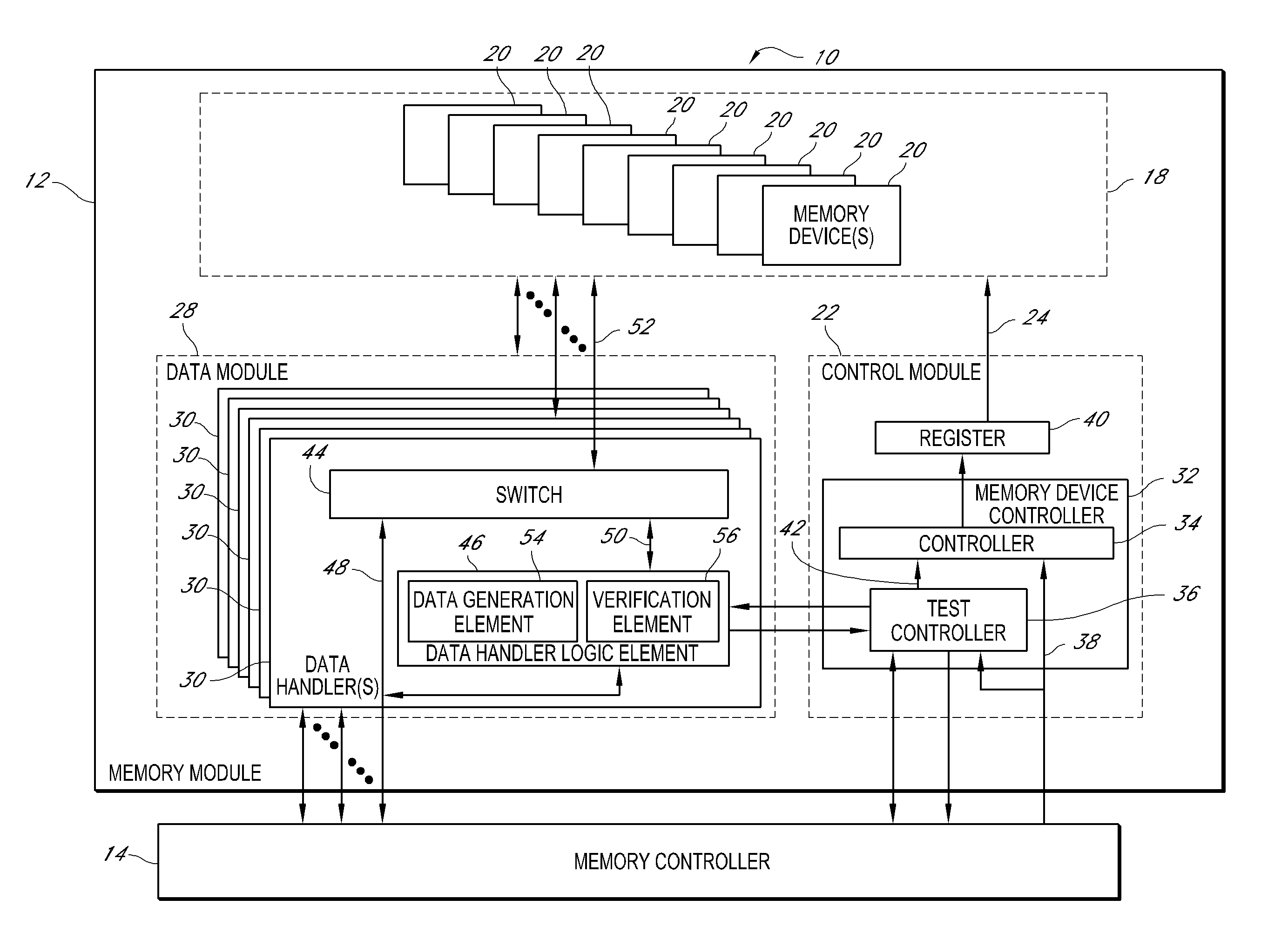
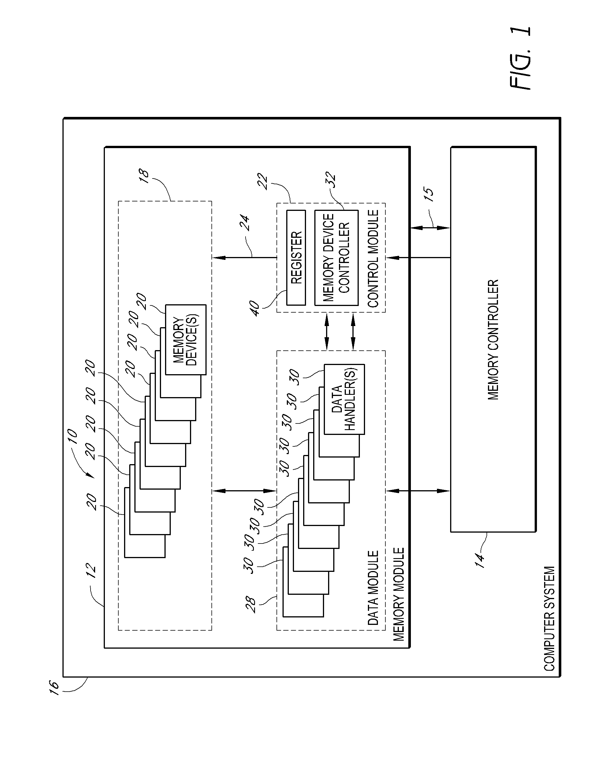
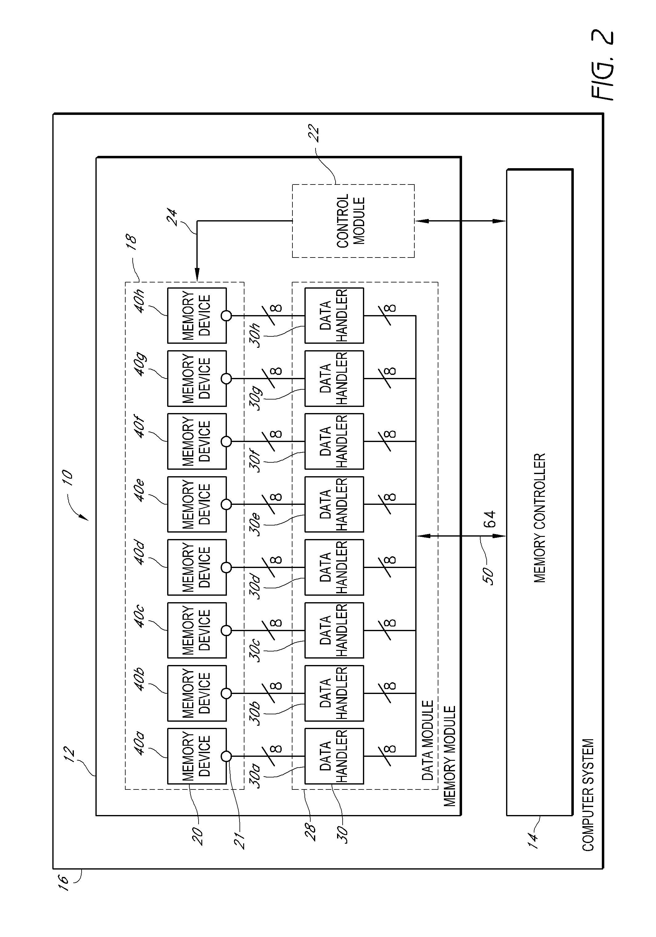
[0018]Certain embodiments described herein present a self-testing electronic system, such as for example, a self-testing electronic memory module. Some embodiments described herein present a self-testing memory module that is populated with ETT DRAM chips. Certain embodiments described herein present a self-testing registered dual in-line memory module (“RDIMM”). Some embodiments described herein present a self-testing RDIMM that does not require any additional pins other than the pins on the standard JEDEC RDIMM connector. For example, the memory module may utilize the address and control signals (e.g., address and control signals generated by the memory module to test the memory module) along with a test signal to enable and execute a self testing function.
[0019]Certain embodiments described herein present a self-testing memory module that includes a control module and a data module which can generate memory addresses and data according to the JEDEC standard memory protocol.
[0020]...
PUM
Abstract
A self-testing memory module includes a printed circuit board configured to be operatively coupled to a memory controller of a computer system and includes a plurality of memory devices on the printed circuit board, each memory device of the plurality of memory devices comprising data, address, and control ports. The memory module also includes a control module configured to generate address and control signals for testing the memory devices. The memory module includes a data module comprising a plurality of data handlers. Each data handler is operable independently from each of the other data handlers of the plurality of data handlers. Each data handler is operatively coupled to a corresponding plurality of the data ports of one or more of the memory devices and is configured to generate data for writing to the corresponding plurality of data ports.
Description
CROSS-REFERENCE TO RELATED APPLICATIONS[0001]The present application is a continuation of U.S. patent application Ser. No. 12 / 422,925, filed Apr. 13, 2009, now U.S. Pat. No. 8,001,434, which claims the benefit of priority from US. Provisional Application No. 61 / 044,801, filed Apr. 14, 2008, US. Provisional Application No. 61 / 044,825, filed Apr. 14, 2008, and US. Provisional Application No. 61 / 044,839, filed Apr. 14, 2008. Each of the foregoing applications is incorporated in their entirety by reference herein. This application is related to U.S. patent application Ser. No. 12 / 422,912, filed on Apr. 13, 2009 and entitled “Self-Adjusting Damper”, which is still pending at the United States Patent and Trademark Office, and to U.S. application Ser. No. 12 / 422,853, filed on Apr. 13, 2009, and entitled “Circuit Providing Load Isolation and Noise Reduction”, now U.S. Pat. No. 8,154,901, both of which are incorporated in their entirety by reference herein.BACKGROUND[0002]1. Field[0003]The p...
Claims
Application Information
Patent Timeline
Application Date:The date an application was filed.
Publication Date:The date a patent or application was officially published.
First Publication Date:The earliest publication date of a patent with the same application number.
Issue Date:Publication date of the patent grant document.
PCT Entry Date:The Entry date of PCT National Phase.
Estimated Expiry Date:The statutory expiry date of a patent right according to the Patent Law, and it is the longest term of protection that the patent right can achieve without the termination of the patent right due to other reasons(Term extension factor has been taken into account ).
Invalid Date:Actual expiry date is based on effective date or publication date of legal transaction data of invalid patent.

