Layered chip package and method of manufacturing same

a chip and chip package technology, applied in the direction of semiconductor devices, electrical equipment, semiconductor/solid-state device details, etc., can solve the problems of increasing the cost of the layered chip package, reducing the distance between the electrodes, and affecting the operation speed of the quick circuit operation

Inactive Publication Date: 2013-01-29
HEADWAY TECH INC +1
View PDF40 Cites 6 Cited by
  • Summary
  • Abstract
  • Description
  • Claims
  • Application Information

AI Technical Summary

Benefits of technology

[0023]It is a first object of the present invention to provide a layered chip package, a composite layered chip package, and methods of manufacturing the same that make it possible that, when a plurality of layered chip packages having the same configuration including a stacked plurality of semiconductor chips are stacked on each other and electrically connected to each other, some of a plurality of signals associated with the semiconductor chips that fall on the same layers in the respective plurality of layered chip packages are easily made different from one layered chip package to another.
[0024]In addition to the first object, it is a second object of the present invention to provide a composite layered chip package and a method of manufacturing the same that make it possible to easily implement a package that provides, even if it includes a malfunctioning semiconductor chip, the same functions as those for the case where no malfunctioning semiconductor chip is included.
[0045]According to the layered chip package, the composite layered chip package, and the methods of manufacturing the same of the present invention, the plurality of pairs of the first and second terminals of the layered chip package (subpackage) include the plurality of non-overlapping terminal pairs. Consequently, according to the present invention, when a plurality of layered chip packages (subpackages) having the same configuration are stacked on each other and electrically connected to each other, some of a plurality of signals associated with the semiconductor chips that fall on the same layers in the respective plurality of layered chip packages (subpackages) can easily be made different from one layered chip package (subpackage) to another.
[0046]According to the composite layered chip package and the methods of manufacturing the same of the present invention, a plurality of subpackages and an additional portion are stacked, and the additional portion is electrically connected to any of the plurality of subpackages. This makes it possible to easily implement a package that is capable of providing, even if it includes a malfunctioning semiconductor chip, the same functions as those for the case where no malfunctioning semiconductor chip is included.

Problems solved by technology

The wire bonding method has the problem that it is difficult to reduce the distance between the electrodes so as to avoid contact between the wires, and the problem that the high resistances of the wires hamper quick circuit operation.
Unfortunately, however, the through electrode method requires a large number of steps for forming the through electrodes in chips, and consequently increases the cost for the layered chip package.
Consequently, voids or keyholes are prone to occur in the through electrodes due to poor filling of the holes with metal.
This tends to reduce the reliability of wiring formed by the through electrodes.
When the vertically adjacent chips are joined to each other at high temperatures, however, misalignment between the vertically adjacent chips can occur due to expansion and contraction of the chips, which often results in electrical connection failure between the vertically adjacent chips.
The manufacturing method disclosed in U.S. Pat. No. 5,953,588 requires a large number of steps and this raises the cost for the layered chip package.
This is also a factor that raises the cost for the layered chip package.
With the multilayer module disclosed in U.S. Pat. No. 7,127,807 B2, it is impossible to increase the proportion of the area occupied by the electronic element in each active layer, and consequently it is difficult to achieve higher integration.
Suppose, however, that a chip including a control circuit and a plurality of memory cells has become defective due to, for example, a wiring failure of the control circuit, and the chip cannot function normally even by employing the redundancy technique.
In such a case, the defective chip is no longer usable.
While the defective chip can be replaced with a conforming one, it increases the cost for the layered chip package.
This can cause the problem of complicated wiring of the memory device including the plurality of layered chip packages.
Disabling access to a defective chip in a layered chip package, however, gives rise to the following two problems.
A first problem is that the defective chip is electrically connected to a plurality of terminals of the layered chip package by wiring, and such a connection can possibly cause malfunction of the layered chip package.
A second problem is that, for a layered chip package that includes a predetermined number of chips and is able to implement a memory device having a desired memory capacity when all the chips included in the layered chip package are conforming, simply disabling access to any defective chip included in the layered chip package is not sufficient for implementing the memory device having the desired memory capacity.

Method used


Image

  • Layered chip package and method of manufacturing same
  • Layered chip package and method of manufacturing same
  • Layered chip package and method of manufacturing same

Examples


first embodiment

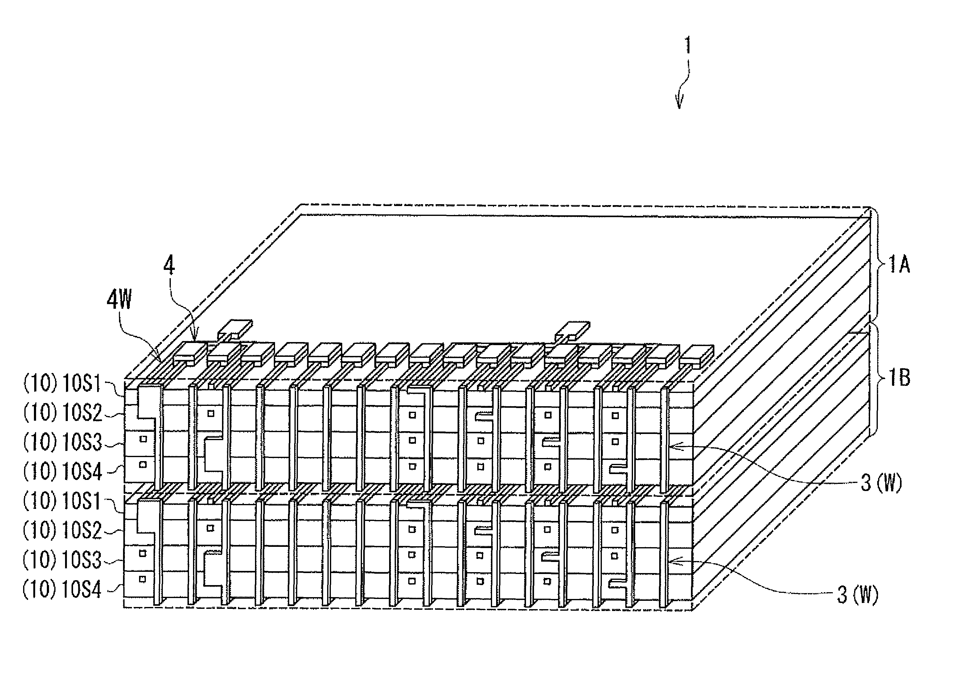
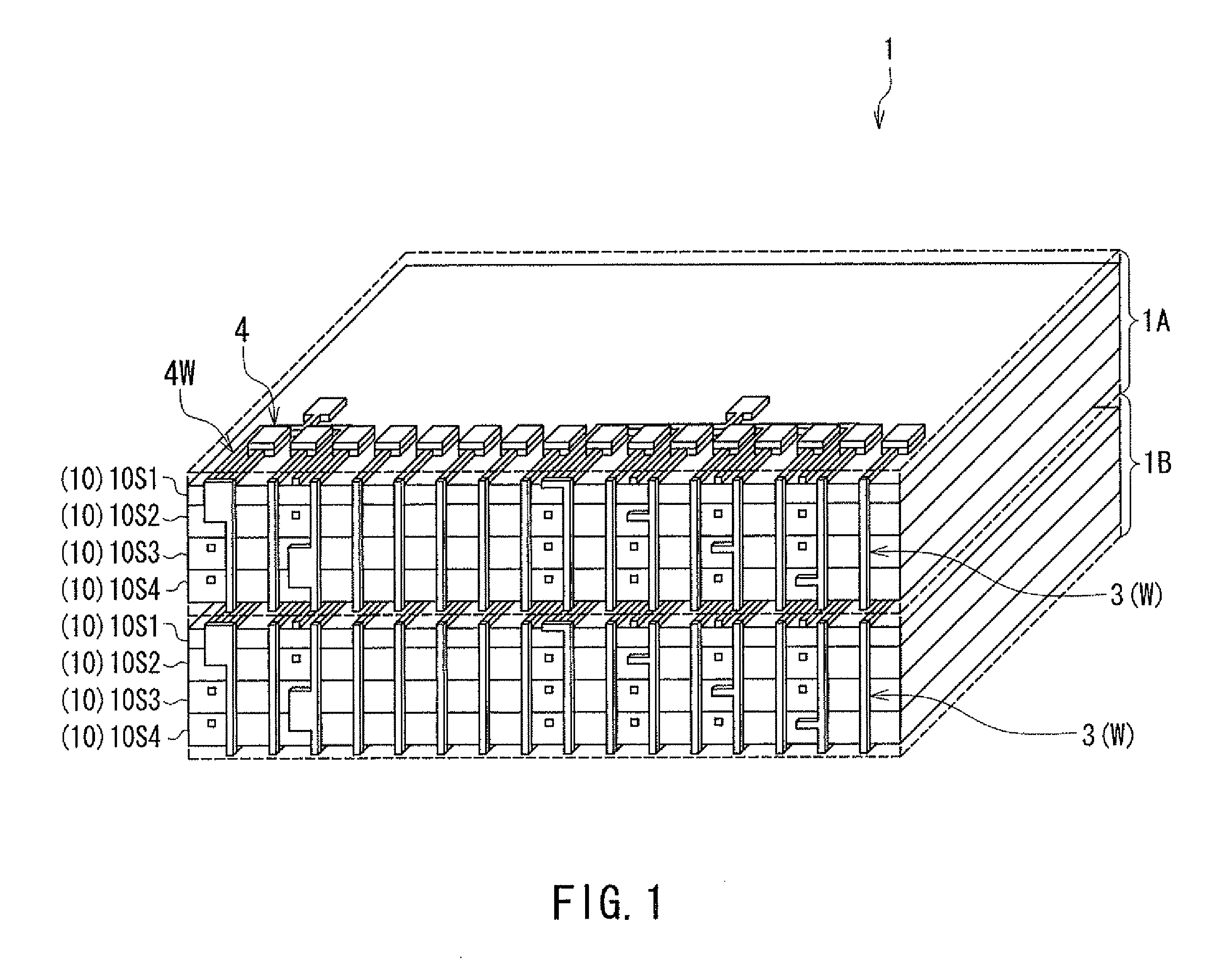
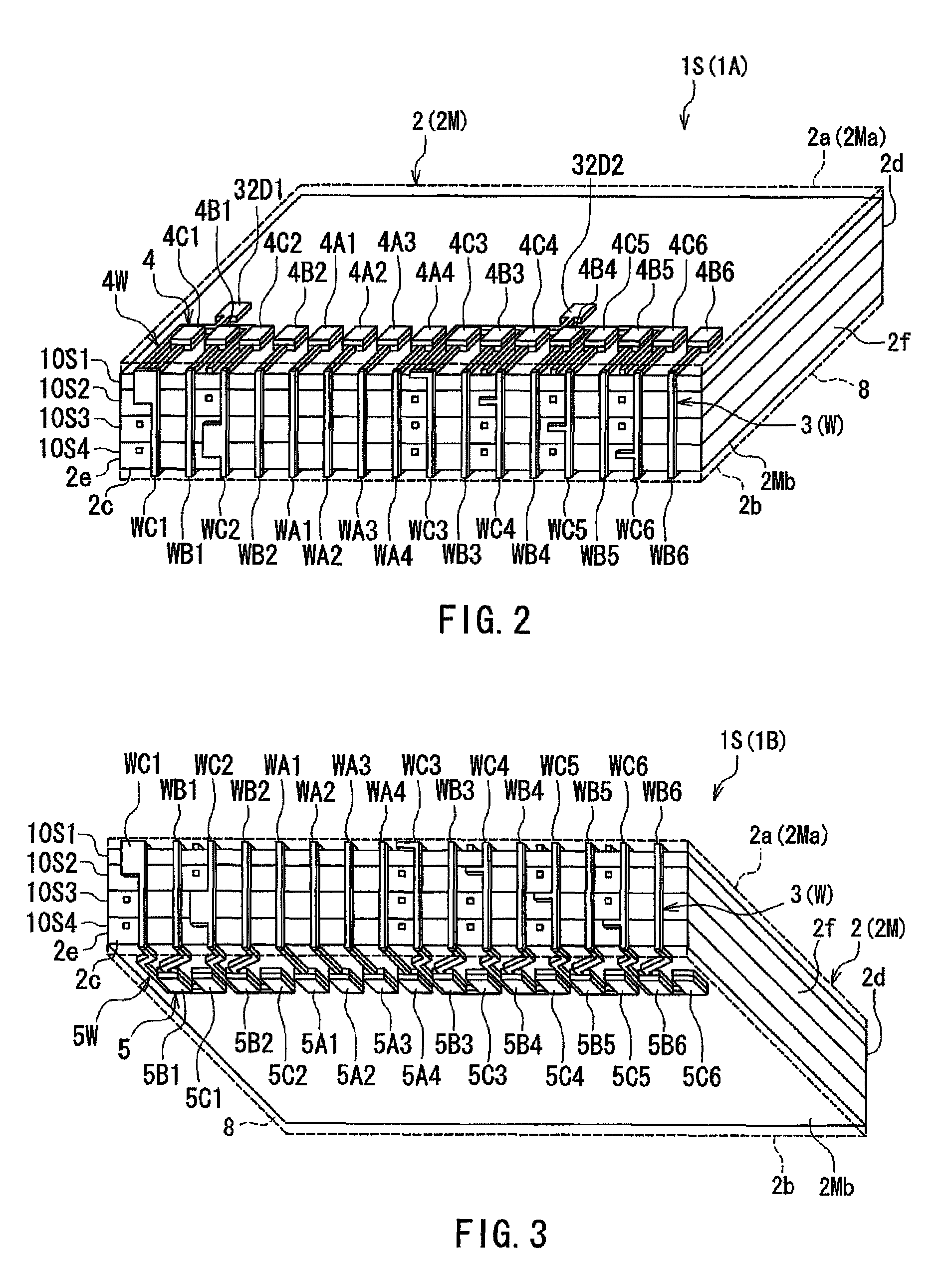
[0111]Preferred embodiments of the present invention will now be described in detail with reference to the drawings. First, reference is made to FIG. 1 to FIG. 6 to describe the configurations of a layered chip package and a composite layered chip package according to a first embodiment of the invention. FIG. 1 is a perspective view of the composite layered chip package according to the present embodiment. FIG. 2 is a perspective view of the layered chip package according to the present embodiment. FIG. 3 is a perspective view showing the layered chip package of FIG. 2 as viewed from below. FIG. 4 is a plan view showing a layer portion included in the layered chip package of FIG. 2. FIG. 5 is a perspective view of the layer portion shown in FIG. 4. FIG. 6 is a plan view showing a plurality of second terminals and bottom wiring of the layered chip package according to the present embodiment as viewed from above.

[0112]As shown in FIG. 1, the composite layered chip package 1 according ...

second embodiment

[0266]A second embodiment of the invention will now be described. FIG. 47 is a perspective view of a subpackage 1S or a layered chip package according to the second embodiment of the invention. The main body 2 of the subpackage 1S according to the present embodiment includes an interposer layer 15 that is bonded to the bottom surface 2Mb of the main part 2M, i.e., the bottom surface of the lowermost layer portion 10 in the main part 2M. The interposer layer 15 includes a substrate part 15a made of an insulating material, a plurality of second terminals 5, bottom wiring 5W, and an insulating layer 8. The substrate part 15a has a top surface that is in contact with the bottom surface 2Mb of the main part 2M, and a bottom surface opposite to the top surface. The plurality of second terminals 5 and the bottom wiring 5W are disposed on the bottom surface of the substrate part 15a. The insulating layer 8 is disposed around the plurality of second terminals 5 on the bottom surface of the s...

third embodiment

[0269]A third embodiment of the invention will now be described. FIG. 48 is a perspective view of a composite layered chip package according to the present embodiment. FIG. 49 is a perspective view of a layered chip package according to the present embodiment. FIG. 50 is a perspective view showing the layered chip package of FIG. 49 as viewed from below. FIG. 51 is a plan view showing a layer portion included in the layered chip package of FIG. 49. FIG. 52 is a perspective view of the layer portion shown in FIG. 51.

[0270]As shown in FIG. 49 and FIG. 50, the main body 2 of the subpackage 1S or the layered chip package according to the embodiment includes an interposer layer 14 that is bonded to the top surface 2Ma of the main part 2M, i.e., the top surface of the uppermost layer portion 10 in the main part 2M. The interposer layer 14 includes a substrate part 14a made of an insulating material, a plurality of first terminals 4, top wiring 4W, and an insulating layer 9. The substrate ...


PUM


Abstract

A layered chip package includes a main body, and wiring that includes a plurality of wires disposed on a side surface of the main body. The main body includes: a main part including a plurality of layer portions; a plurality of first terminals disposed on the top surface of the main part and connected to the wiring; and a plurality of second terminals disposed on the bottom surface of the main part and connected to the wiring. Each layer portion includes a semiconductor chip. The plurality of second terminals are positioned to overlap the plurality of first terminals as viewed in a direction perpendicular to the top surface of the main body. A plurality of pairs of first and second terminals that are electrically connected via the wires include a plurality of pairs of a first terminal and a second terminal that are positioned not to overlap each other.

Description

BACKGROUND OF THE INVENTION[0001]1. Field of the Invention[0002]The present invention relates to a layered chip package that includes a plurality of semiconductor chips stacked, and to a method of manufacturing the same.[0003]2. Description of the Related Art[0004]In recent years, lighter weight and higher performance have been demanded of portable devices typified by cellular phones and notebook personal computers. Accordingly, there has been a need for higher integration of electronic components for use in the portable devices. With the development of image- and video-related equipment such as digital cameras and video recorders, semiconductor memories of larger capacity and higher integration have also been demanded.[0005]As an example of highly integrated electronic components, a system-in-package (hereinafter referred to as SiP), especially an SiP utilizing a three-dimensional packaging technology for stacking a plurality of semiconductor chips, has attracting attention in rece...

Claims


Application Information

Patent Timeline
Patent Type & Authority Patents(United States)
IPC IPC(8): H01L23/02
CPCH01L23/5382H01L25/0657H01L25/50H01L24/01H01L2225/06527H01L2924/07802H01L2225/06551H01L2924/00
Inventor SASAKI, YOSHITAKAITO, HIROYUKIIKEJIMA, HIROSHIIIJIMA, ATSUSHI
Owner HEADWAY TECH INC
Why Eureka
Try Eureka