Device package, a printed wiring board, and an electronic apparatus with efficiently spaced bottom electrodes including intervals between bottom electrodes of different lengths

a technology of printed wiring and electronic equipment, applied in the direction of printed circuit non-printed electric components association, sustainable manufacturing/processing, final product manufacturing, etc., can solve the problems of increasing dimensions, increasing costs, and difficulty in providing a sufficient number of connections between elements, so as to increase the number of electrode rows and facilitate the making of different, the effect of efficient wiring

Active Publication Date: 2008-04-22
RICOH KK
View PDF23 Cites 8 Cited by
  • Summary
  • Abstract
  • Description
  • Claims
  • Application Information

AI Technical Summary

Benefits of technology

[0013]In the present invention, the intervals between the edges of the pads of the PWB are set to vary corresponding to the arrangement of the electrodes of the device package. Different intervals of the pads provide for different numbers of wires that can be provided between the pads, and a relatively greater interval provides a space for a via (etched pathway). In this manner, a greater number of wires can be provided between the device package and the PWB. For example, the interval between the edges of the electrodes is made to be different by providing no electrodes at a position of an array of electrodes corresponding to an electrode of a lower (inner) sequence (row). Further, the interval between the edges of the electrodes can be easily made different by providing different sizes of the electrodes from place to place. Especially, the intervals between electrodes are made greater on the peripheral side of the array than on the inner side. Given that the number of electrodes inside the array is greater for an array in which the interval is greater on the peripheral side, the greater interval on the peripheral side is required to provide a sufficient space for the wires to access the peripheral positions. In addition, the same effect is obtained by providing a smaller number of electrodes on the inner side, and making the interval on the peripheral side smaller. Further, spaces for vias can be obtained by sparsely arranging electrodes near the center of the device package, the vias being for the central electrodes to access the peripheral positions, while outer electrodes access the peripheral positions using the surface of the PWB. Accordingly, electrodes immediately adjacent to the electrodes that are pulled out using vias of the PWB can be arranged with smaller intervals, given that they do not have to be spaced so as to provide a wiring space between corresponding pads, and do not require vias. Compared with the interval between the electrodes immediately adjacent to the electrodes that are pulled out using the vias, the interval to the electrodes of the next sequence (row) is made greater such that the vias can be provided. In this manner, efficient wiring is realized. In addition, in the case that the electrodes are sparse in the central part of the device package, wires of the inner electrodes of the device packages (BGA, etc.) are pulled out using the surface of the PWB. For this reason, from the relations between the pads and the corresponding electrodes that are located immediately before and after the electrodes that are pulled out using the vias, the same effect is acquired. Further, it is also possible to increase the number of electrode rows by changing (narrowing) the interval between the electrode rows. Further, the present invention provides an electronic apparatus using the device package and the PWB according to the present invention, which realizes reductions in cost and dimensions.

Problems solved by technology

However, it is often difficult to provide a sufficient number of connections between elements within a desired small space.
Further, it is predicted that connections between the elements will become impossible in the near future even if the build-up technology is used.
Nevertheless, with the conventional technology, the auxiliary device package for wiring is additionally required, and an increased number of layers in the PWB is required, which raise costs and increase dimensions.

Method used


Image

  • Device package, a printed wiring board, and an electronic apparatus with efficiently spaced bottom electrodes including intervals between bottom electrodes of different lengths
  • Device package, a printed wiring board, and an electronic apparatus with efficiently spaced bottom electrodes including intervals between bottom electrodes of different lengths
  • Device package, a printed wiring board, and an electronic apparatus with efficiently spaced bottom electrodes including intervals between bottom electrodes of different lengths

Examples


Embodiment Construction

[0021]In the following, embodiments of the present invention are described with reference to the accompanying drawings.

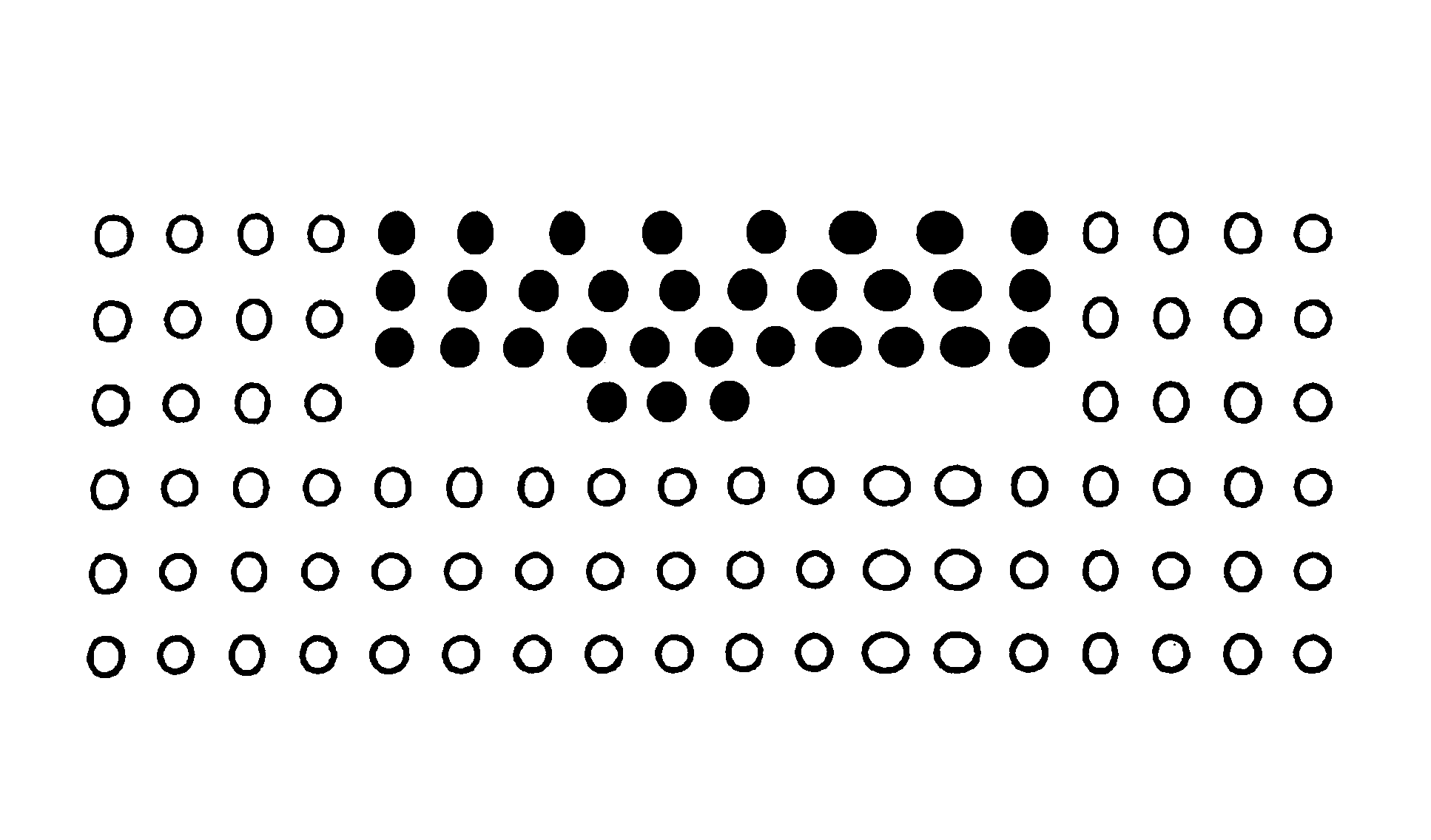
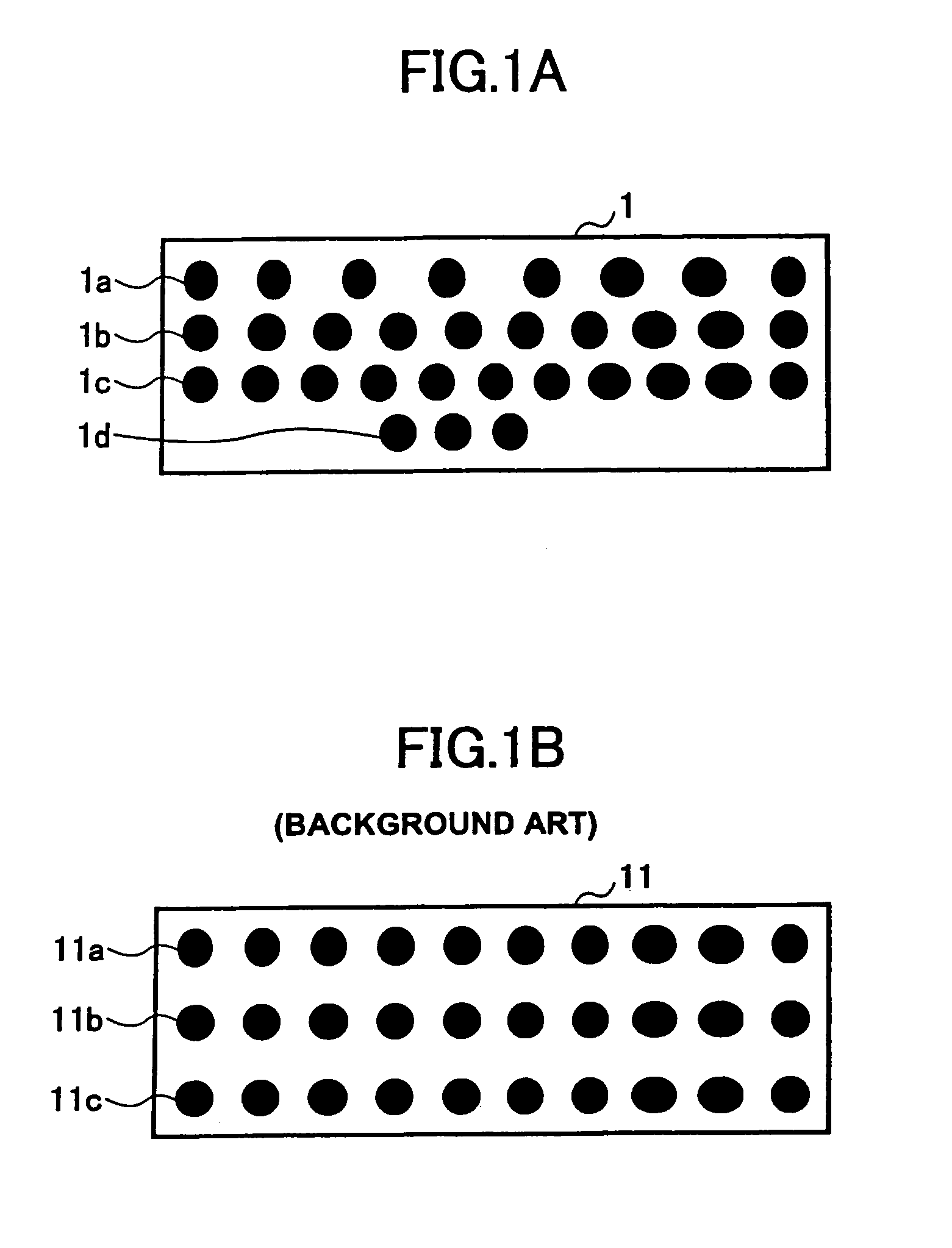
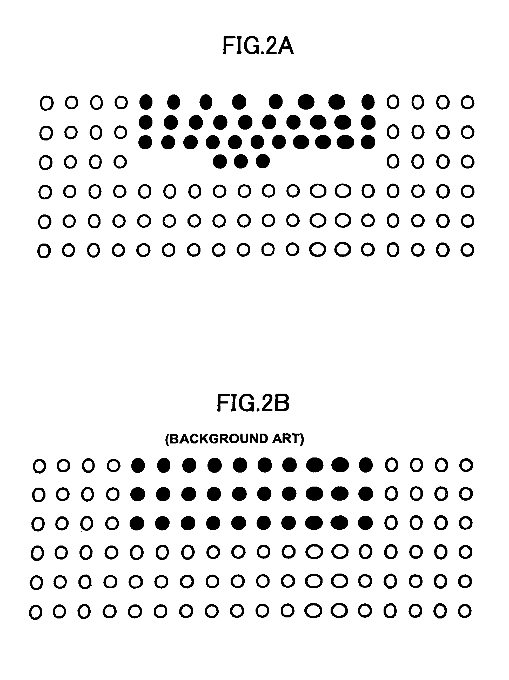
[0022]FIGS. 1A and 1B give layout diagrams showing examples of device package bottom electrode arrangements according to the present invention, and according to conventional practice, and FIGS. 2A and 2B give layout diagrams showing printed wiring board (PWB) pad arrangements according to the present invention, and according to the conventional practice.

[0023]A device package 1 shown in FIG. 1A is mounted on a PWB shown in FIG. 2A. A device package 11 shown in FIG. 1B is mounted on a PWB shown in FIG. 2B.

[0024]For a given wiring density (a line width and an interval) of a PWB, the number of wires that can be provided between the pads of the PWB depends on the distance between the edges of the electrodes of the device package, the pads corresponding to the electrodes of the device package for surface mounting to the PWB. Further, since it is necessary to provide a ce...


PUM


Abstract

A device package, such as a BGA, to be mounted on a printed wiring board (PWB) is disclosed. The bottom electrodes of the device package are arranged in an array such that intervals between the edges of the bottom electrodes become different from place to place. The intervals may be set wider at the peripheral positions of the bottom electrodes. The PWB includes pads that are located at positions corresponding to the bottom electrodes.

Description

BACKGROUND OF THE INVENTION[0001]1. Field of the Invention[0002]The present invention generally relates to semiconductor integrated circuit technology, and especially relates to a technology of efficiently providing wires from a device package having bottom electrodes, such as a BGA (Ball Grid Array), to a printed wiring board (PWB), on which the device package is mounted.[0003]2. Description of the Related Art[0004]Device packages, i.e., semiconductor integrated circuits, are required to provide a great number of pins in small dimensions for high-density mounting. In concert with the miniaturization (high-density) of the device packages, high-density wiring of the PWB is required. However, it is often difficult to provide a sufficient number of connections between elements within a desired small space.[0005]In order to pull out wiring from the inner positions of the device package (an electronic part) having bottom electrodes, such as a BGA, the number of layers of the PWB must be ...

Claims


Application Information

Patent Timeline
Patent Type & Authority Patents(United States)
IPC IPC(8): H01L23/48H05K3/34H01L23/12H01L23/50H05K1/11H05K1/18
CPCH01L23/50H05K1/111H05K3/3436H05K2201/094H01L2924/0002H05K2201/10734H01L2924/00Y02P70/50
Inventor YASHIRO, AKIRA
Owner RICOH KK
Why Eureka
Try Eureka