Resist pattern protection technique for double patterning application

a protection technique and pattern technology, applied in the field of resist pattern protection techniques for double patterning applications, can solve the problems of high manufacturing cost and complex prior art double patterning process

Inactive Publication Date: 2013-03-12
WESTERN DIGITAL TECH INC
View PDF12 Cites 155 Cited by
  • Summary
  • Abstract
  • Description
  • Claims
  • Application Information

AI Technical Summary

Problems solved by technology

These prior art double patterning processes are complex, involving two or more pattern transfer operations involving RIE or mill / lift-off steps.
The complexity inherent in the prior art double patterning processes makes these approaches expensive in manufacturing, and process variations can be large from the double lithography and double pattern transfer operations.

Method used


Image

  • Resist pattern protection technique for double patterning application
  • Resist pattern protection technique for double patterning application
  • Resist pattern protection technique for double patterning application

Examples


Embodiment Construction

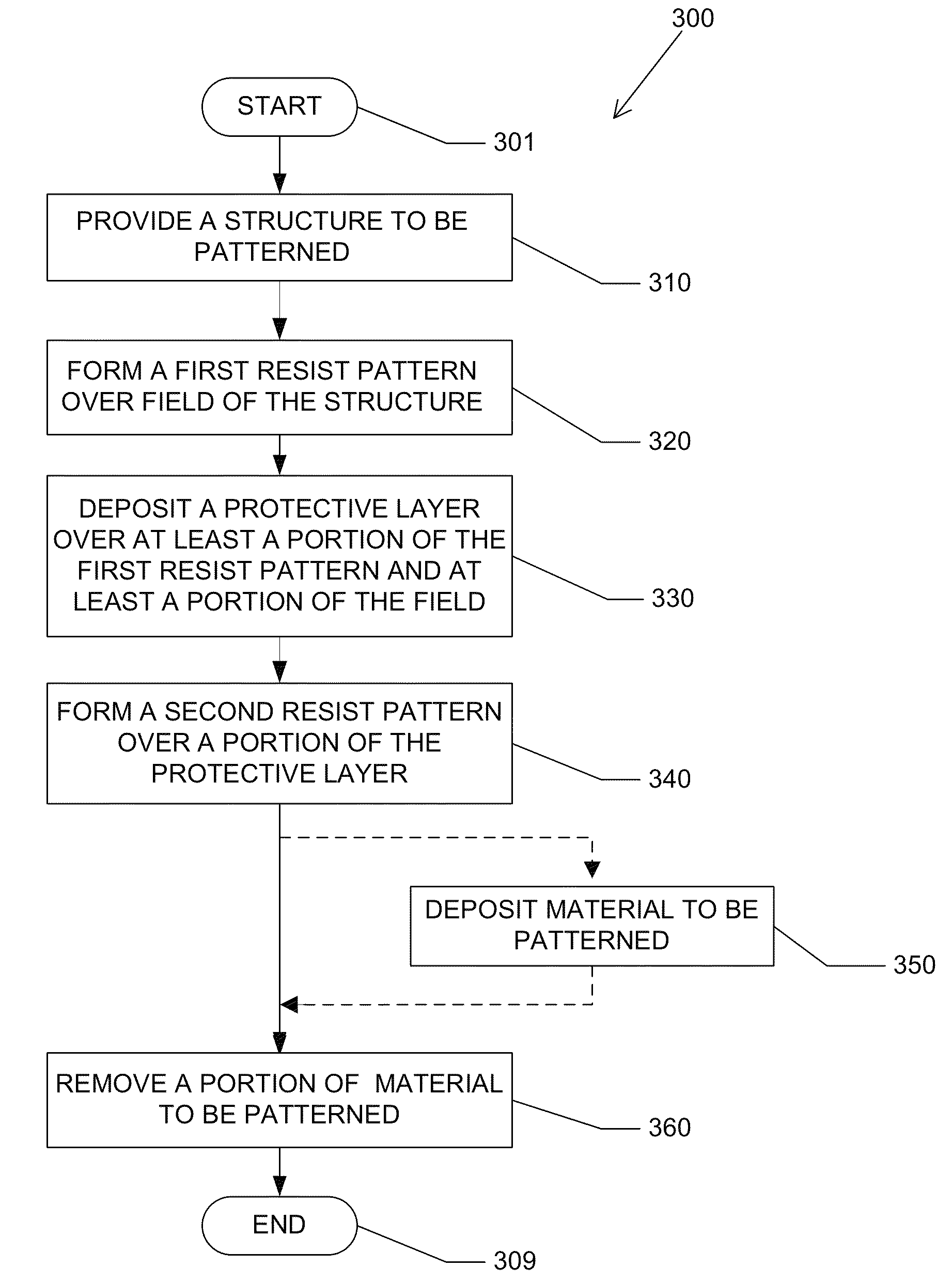
[0016]In the following detailed description, numerous specific details are set forth to provide a full understanding of the present invention. It will be apparent, however, to one ordinarily skilled in the art that the present invention may be practiced without some of these specific details. In other instances, well-known structures and techniques have not been shown in detail to avoid unnecessarily obscuring the present invention.

[0017]FIG. 3 is a flowchart illustrating an exemplary double patterning process 300 that can be used in the semiconductor industry to produce a patterned structure such as structure 409 of FIG. 4 or structure 609 of FIG. 6 according to one aspect of the subject disclosure. For the sake of clarity only with no intention of limiting the subject disclosure in any way, the process 300 will be described below with frequent references to various intermediate and final structures shown in FIG. 4 and some references to intermediate and final structures shown in F...


PUM

PropertyMeasurementUnit
thicknessaaaaaaaaaa
thicknessaaaaaaaaaa
shapeaaaaaaaaaa

Abstract

Methods of patterning a material are disclosed. A first resist pattern is formed on a field. A protective layer is formed over the first resist pattern and at least a portion of the field. A second resist pattern is formed over a portion of the protective layer. A portion of a material to be patterned deposited adjacent to the first and second resist patterns is removed.

Description

FIELD OF THE INVENTION[0001]The present invention generally relates to double patterning processes for producing patterned thin-film structures and, in particular, relates to resist pattern protection techniques for double patterning applications.BACKGROUND OF THE INVENTION[0002]Double patterning processes are used in the semiconductor industry to practically double the photolithographic resolution for a dense line / spacing patterning. FIG. 1 illustrates an example of such a prior art double patterning process used in the semiconductor industry to produce a densely patterned structure. The prior art process involves: 1) providing a structure 101 having a substrate 110, a silicon (Si) layer 120, and a hard mask (HM) layer 130; 2) performing a first lithography operation to form a first resist pattern 140 on the HM layer 130; 3) performing a first pattern transfer operation (e.g., a reactive ion etching (RIE)) to form a HM 132 by removing a portion of the HM material not covered by the...

Claims


Application Information

Patent Timeline
Patent Type & Authority Patents(United States)
IPC IPC(8): B44C1/22
CPCG11B5/1278G11B5/3163H01L21/0273H01L21/0332H01L21/0337
Inventor WAN, DUJIANGSUN, HAIYUAN, HONGPINGWANG, LINGZENG, XIANZHONG
Owner WESTERN DIGITAL TECH INC
Why Eureka
Try Eureka