Liquid crystal display manufacturing method, liquid crystal display, and electronic apparatus
a manufacturing method and liquid crystal technology, applied in the field of liquid crystal display, can solve problems such as complicated structure of display, and achieve the effects of preventing the spread of seal material, reducing the thickness of the display, and reducing the size of the display
- Summary
- Abstract
- Description
- Claims
- Application Information
AI Technical Summary
Benefits of technology
Problems solved by technology
Method used
Image
Examples
first embodiment
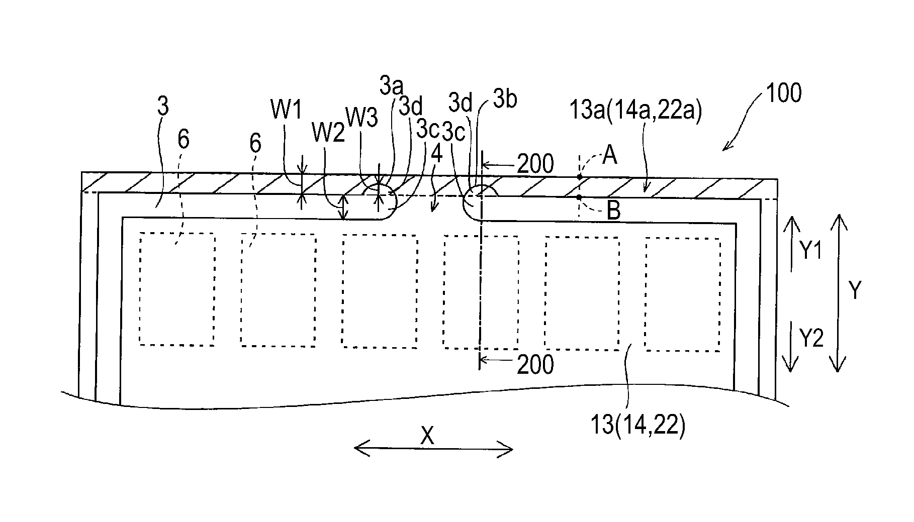
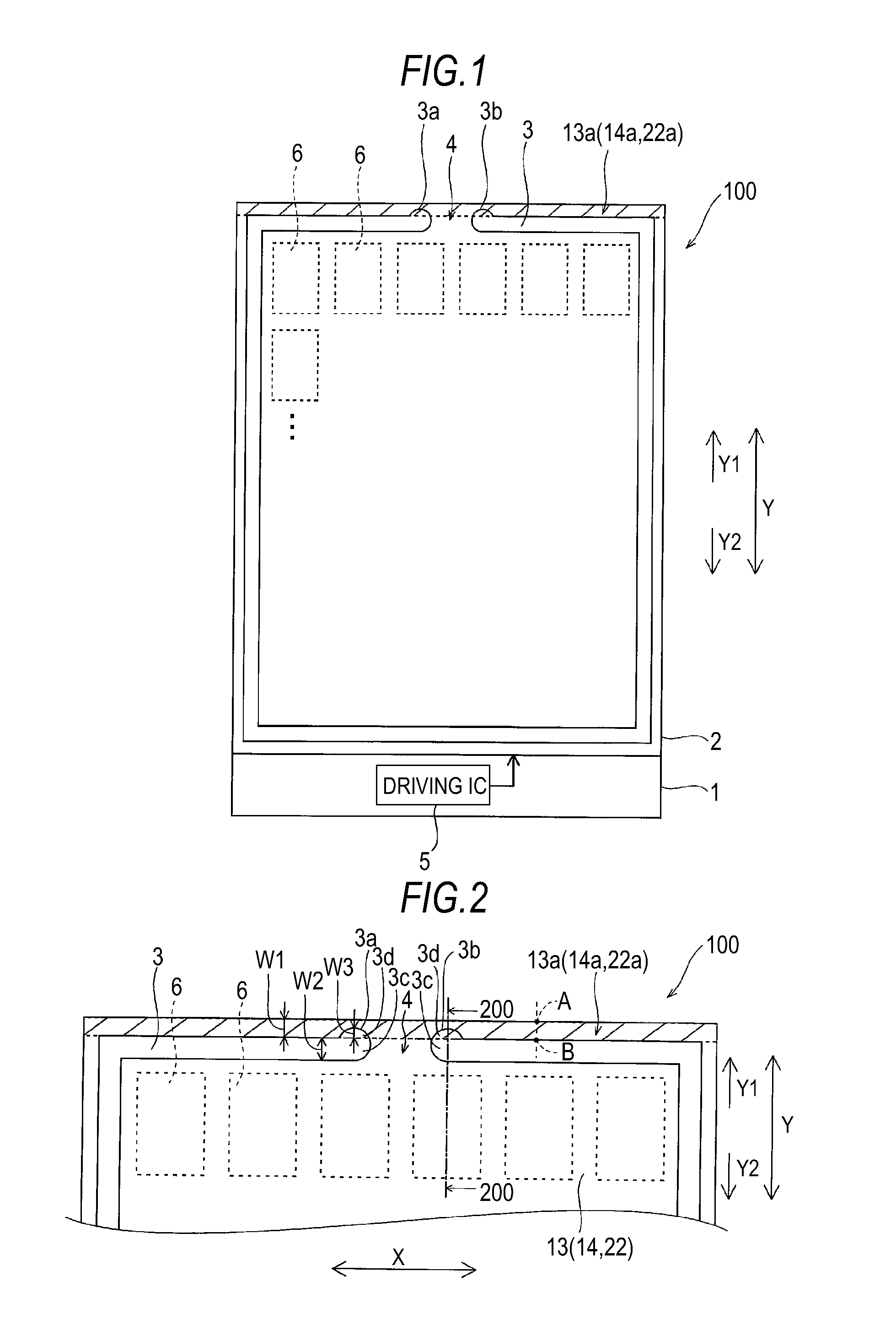
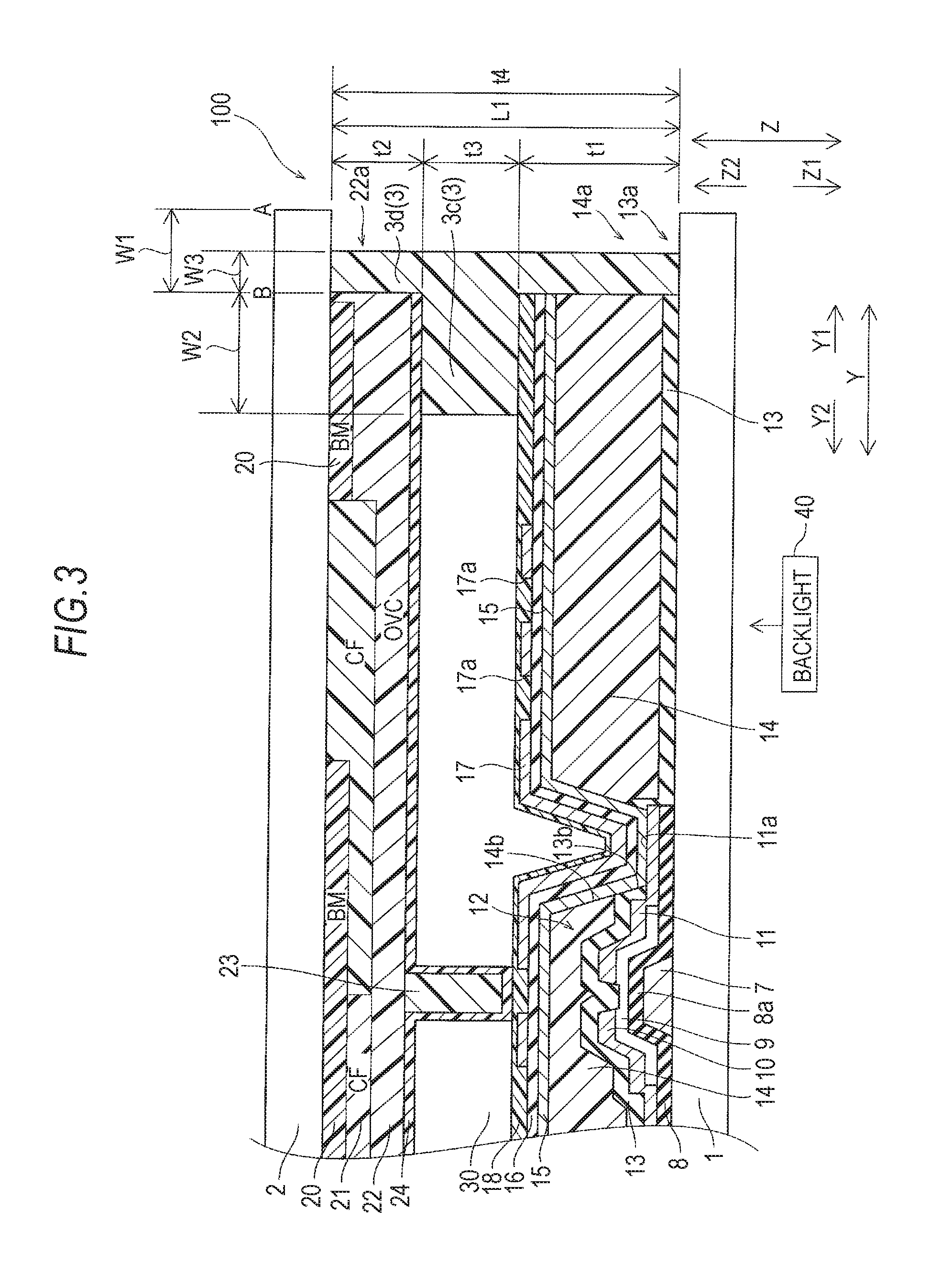
[0042]A configuration of a liquid crystal display 100 according to a first embodiment will now be described with reference to FIGS. 1 to 3. The first embodiment is an application of the application to a lateral field mode liquid crystal display 100.
[0043]As shown in FIG. 1, the liquid crystal display 100 according to the first embodiment includes a TFT substrate 1 having a substantially rectangular shape and an opposite substrate 2 having a substantially rectangular shape. The TFT substrate 1 is an example of the “first substrate” described above, and the opposite substrate 2 is an example of the “second substrate” described above. The TFT substrate 1 and the opposite substrate 2 are combined using a seal material 3. The seal material 3 is applied to the TFT substrate 1 or the opposite substrate 2 along the periphery thereof using a dispenser. The seal material 3 is applied to a surface of the TFT substrate 1 or the opposite substrate 2 such that the application is started at a star...
second embodiment
[0073]A second embodiment will now be described with reference to FIG. 15. The second embodiment is different from the first embodiment as follows. The relief portions 13a, 14a, and 22a of the first embodiment are provided throughout the side of an area including panel regions on which the liquid crystal injection port is provided, whereas relief portions 113a, 114a, and 122a according to the second embodiment are formed in regions on the side of an area including panel regions other than a region in which a liquid crystal injection port 4 is provided.
[0074]In a liquid crystal display 100a according to the second embodiment, as shown in FIG. 15, the relief portions 113a, 114a, and 122a are provided in regions (indicated by oblique lines in FIG. 15) of a passivation film 13, a leveling film 14, and an overcoat layer 22, respectively, other than a region of the associated with a liquid crystal injection port 4 near the periphery of the display on the side thereof indicated by the arro...
third embodiment
[0077]A third embodiment will now be described with reference to FIG. 16. The third embodiment is different from the first embodiment as follows. The relief portions 13a, 14a, and 22a of the first embodiment are provided throughout the side of the area including panel regions on which the liquid crystal injection port 4 is provided, whereas relief portions 213a, 214a, and 222a according to the third embodiment are formed by removing regions of a passivation film 13, a leveling film 14, and an overcoat layer 22 associated with a start point 3a and an end point 3b of a seal material 3.
[0078]In a liquid crystal display 100b according to the third embodiment, as shown in FIG. 16, relief portions 213a, 214a, and 222a are provided only in respective regions (indicated by oblique lines in FIG. 16) of a passivation film 13, a leveling film 14, and an overcoat layer 22 associated with a start point 3a and an end point 3b of a seal material 3 in the neighborhood of the periphery of the displa...
PUM
 Abstract
Description
Claims
Application Information
 - R&D
- Intellectual Property
- Life Sciences
- Materials
- Tech Scout
- Unparalleled Data Quality
- Higher Quality Content
- 60% Fewer Hallucinations
Browse by: Latest US Patents, China's latest patents, Technical Efficacy Thesaurus, Application Domain, Technology Topic, Popular Technical Reports.
© 2025 PatSnap. All rights reserved.Legal|Privacy policy|Modern Slavery Act Transparency Statement|Sitemap|About US| Contact US: help@patsnap.com


