Power semiconductor apparatus having a silicon power semiconductor device and a wide gap semiconductor device

a technology of power semiconductor and semiconductor device, which is applied in the direction of semiconductor devices, electrical equipment, basic electric elements, etc., can solve the problems of large leakage current of power semiconductor device using sic or gan as the base substance, difficult to accurately measure leakage current characteristics of power semiconductor device, etc., to achieve suppressed heat conduction between both power semiconductor devices and accurate measurement

Inactive Publication Date: 2013-05-14
HITACHI LTD
View PDF7 Cites 7 Cited by
  • Summary
  • Abstract
  • Description
  • Claims
  • Application Information

AI Technical Summary

Benefits of technology

[0012]Since a power semiconductor device using Si as a base substance and a power semiconductor device using a semiconductor having an energy bandgap wider than the energy bandgap of Si are mounted on respective insulated metal substrates, and in addition, since the insulated metal substrates are mounted on respective heat dissipation metal bases, a heat conduction between both the power semiconductor devices can be suppressed. Furthermore, since the positive and the negative main terminals of the power semiconductor device using Si are electrically separated from those of the power semiconductor device using a semiconductor having an energy bandgap wider than the energy bandgap of Si, leakage currents of both power semiconductor devices can be accurately measured.

Problems solved by technology

In addition, a leakage current of the power semiconductor device using SiC or GaN as the base substance is large due to the effect of crystal defects.
Especially, a leakage current of a Schottky-barrier diode using SiC or GaN becomes large.
Therefore, it is difficult to accurately measure leakage current characteristics of the power semiconductor device using Si as the base substance.

Method used


Image

  • Power semiconductor apparatus having a silicon power semiconductor device and a wide gap semiconductor device
  • Power semiconductor apparatus having a silicon power semiconductor device and a wide gap semiconductor device
  • Power semiconductor apparatus having a silicon power semiconductor device and a wide gap semiconductor device

Examples


first embodiment

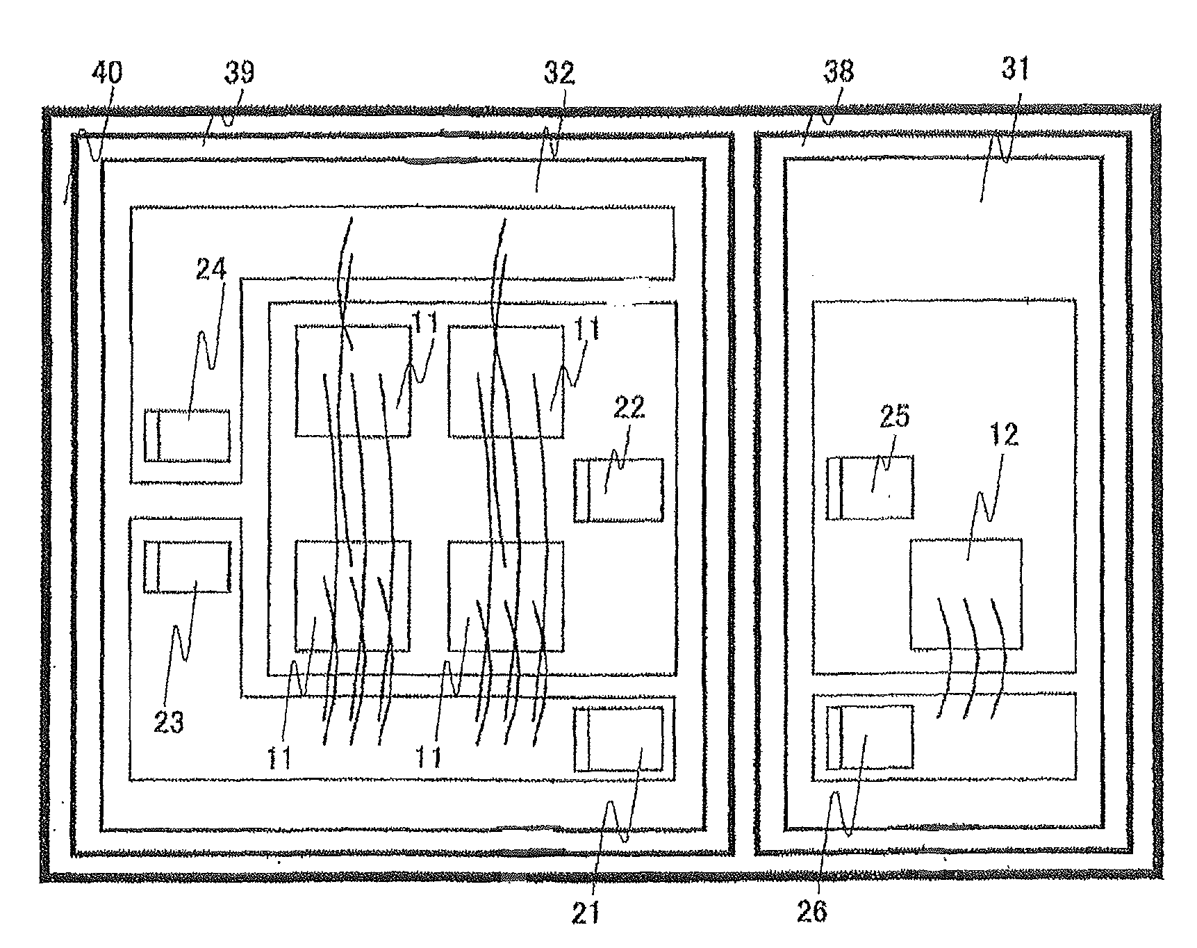
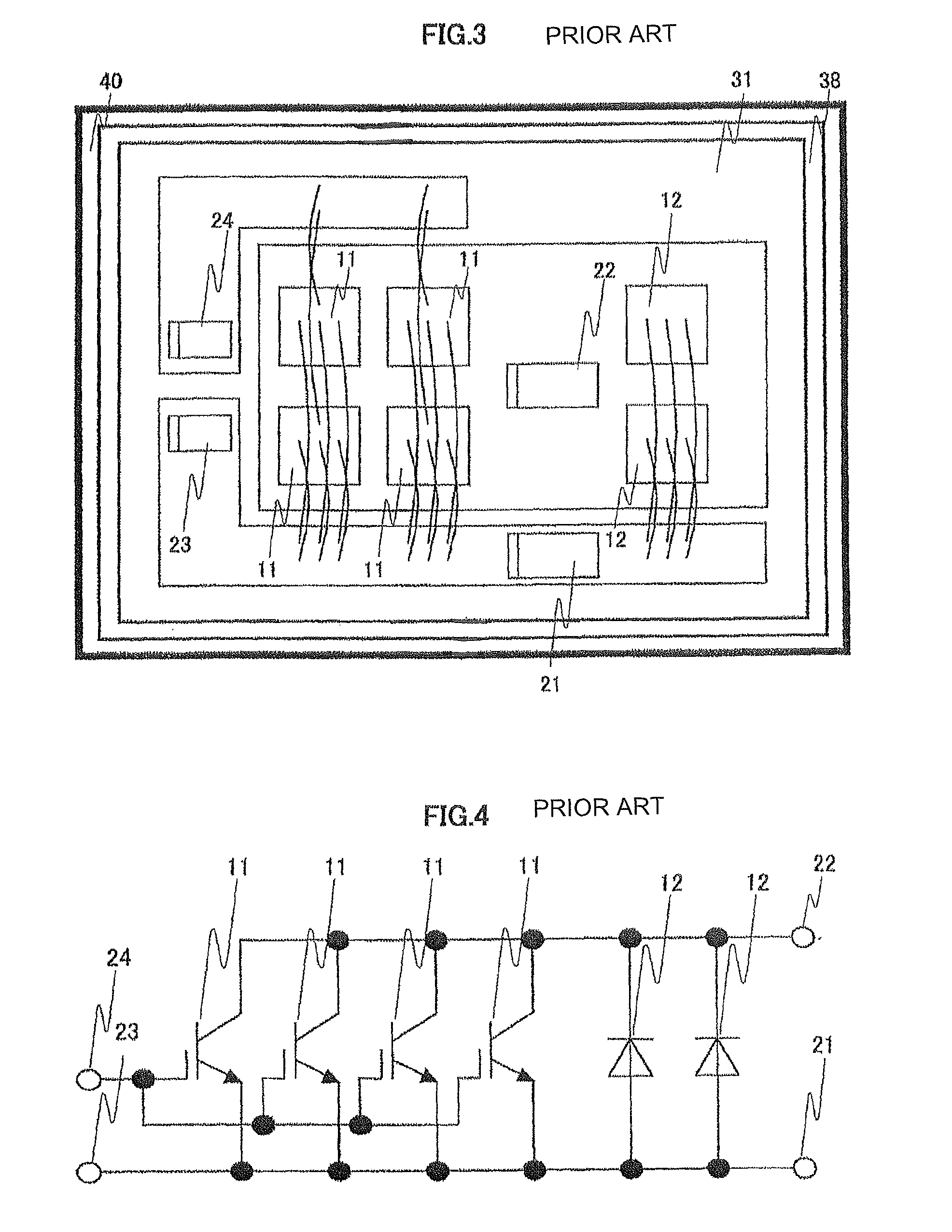
[0026]FIG. 3 shows a mounting arrangement example of a conventional power semiconductor apparatus. In a mounting method of the conventional power semiconductor apparatus, the Si-IGBT 11 and the SiC-SBD 12 are mounted on the same insulated metal substrate 31. In this case, due to a heat generation of the Si-IGBT 11 and the SiC-SBD 12, a heat is likely to be transferred to each of the chips via the insulated metal substrate 31. Therefore, although a SiC-SBD generally can operate at a higher temperature in comparison with a Si-IGBT, an operation temperature of the SiC-SBD 12 is limited to that of the Si-IGBT 11. On the other hand, in the first embodiment, since the heat dissipation metal base 39 including the insulated metal substrate 32 on which the Si-IGBT 11 is mounted is separated from the heat dissipation metal base 38 including the insulated metal substrate 31 on which the SiC-SBD 12 is mounted, the SiC-SBD 12 can be operated at a high temperature without limitation of the operat...

second embodiment

[0037]FIG. 9 shows a power loss reduction effect when a power semiconductor apparatus according to the first or the present invention is applied to an inverter, which is an electric power conversion system. A calculation example of power loss of a conventional inverter is shown on the left in FIG. 9. An inverter loss is mainly caused in a switching device and a diode. A loss caused by the switching device is expressed by a sum of a conduction loss, a turn-ON loss and a turn-OFF loss, and a loss caused by the diode is expressed by a sum of a conduction loss and a recovery loss. Meanwhile, in the conventional inverter, a Si-IGBT and a PiN diode of Silicon (hereinafter, referred to as Si-PiN diode) are used. The ratio of a conduction loss to a switching loss varies depending on a frequency of the inverter. However, the ratio of an IGBT loss to a diode loss is approximately 2:1 even if the frequency of the inverter is varied. Therefore, if the ratio of an IGBT chip size to a diode chip ...

third embodiment

[0042]FIG. 11 shows a mounting arrangement of a power semiconductor apparatus according to the is present invention. A size of the power semiconductor apparatus was reduced by reducing a device area of the IGBT that is a power semiconductor device using Si as a base substance.


PUM


Abstract

A power semiconductor apparatus which is provided with a first power semiconductor device using Si as a base substance and a second power semiconductor device using a semiconductor having an energy bandgap wider than the energy bandgap of Si as a base substance, and includes a first insulated metal substrate on which the first power semiconductor device is mounted, a first heat dissipation metal base on which the first insulated metal substrate is mounted, a second insulated metal substrate on which the second power semiconductor device is mounted, and a second heat dissipation metal base on which the second insulated metal substrate is mounted.

Description

CROSS REFERENCE TO RELATED APPLICATIONS[0001]This application claims the foreign priority benefit under Title 35, United States Code, §119(a)-(d) of Japanese Patent Application No. 2009-080850, filed on Mar. 30, 2009, the contents of which are hereby incorporated by reference.FIELD OF THE INVENTION[0002]The present invention relates to a power semiconductor apparatus which is provided with a power semiconductor device using Si as a base substance and a power semiconductor device using a wide-gap semiconductor as a base substance.DESCRIPTION OF RELEVANT ART[0003]A wide-gap semiconductor device using silicon carbide (SiC) or gallium nitride (GaN) which has a wider energy bandgap than that of silicon (Si) is getting a lot of attention. Since these materials have a breakdown field ten times higher than that of Si and thereby a drift layer for securing a breakdown voltage can be made thin about 1 / 10 in comparison with Si, a lowering of ON-voltage of a power semiconductor device and opera...

Claims


Application Information

Patent Timeline
Patent Type & Authority Patents(United States)
IPC IPC(8): H01L27/06
CPCH01L25/18H01L25/115H01L29/872H01L29/7393H01L29/2003H01L29/1608H01L29/16H01L27/06H01L25/072H01L2924/13062H01L2924/1305H01L2924/12032H01L2924/13091H01L2224/48227H01L2224/49111H01L2924/13055H01L2924/30107H01L2924/00H01L2224/48137H01L2224/49113H01L2224/48111
Inventor ISHIKAWA, KATSUMIOGAWA, KAZUTOSHI
Owner HITACHI LTD
Why Eureka
Try Eureka