IR sensing device

a sensing device and infrared radiation technology, applied in the field of infrared radiation sensing devices, can solve the problems of deteriorating the malleability and flexibility of optical coatings, the inability of optical coatings to be coated on the lenses nor the optical sensors, and the inability to achieve high cost and production difficulty

Active Publication Date: 2013-05-21
PIXART IMAGING INC
View PDF10 Cites 0 Cited by
  • Summary
  • Abstract
  • Description
  • Claims
  • Application Information

AI Technical Summary

Benefits of technology

[0006]A common method for preventing these difficulties is to use a thin-film optical coating on glass to create an optical element which blocks visible light (typically from 400 nm to 780 nm) and passes the IR. However, to block light with such wide range (400 nm to 780 nm), the number of the layers of the optical coating is larger, e.g. 45. Since the number of the layers of the optical coating has to be so large to achieve the capability of filtering out the non-IR, which deteriorates the malleability and the flexibility of the optical coating, the optical coating can not be coated on the lens nor the optical sensor consequently. Therefore, the conventional IR sensing device realized with the optical coating comes with high cost and difficulty for production, which is inconvenient.

Problems solved by technology

Since the number of the layers of the optical coating has to be so large to achieve the capability of filtering out the non-IR, which deteriorates the malleability and the flexibility of the optical coating, the optical coating can not be coated on the lens nor the optical sensor consequently.
Therefore, the conventional IR sensing device realized with the optical coating comes with high cost and difficulty for production, which is inconvenient.

Method used


Image

  • IR sensing device
  • IR sensing device
  • IR sensing device

Examples


first embodiment

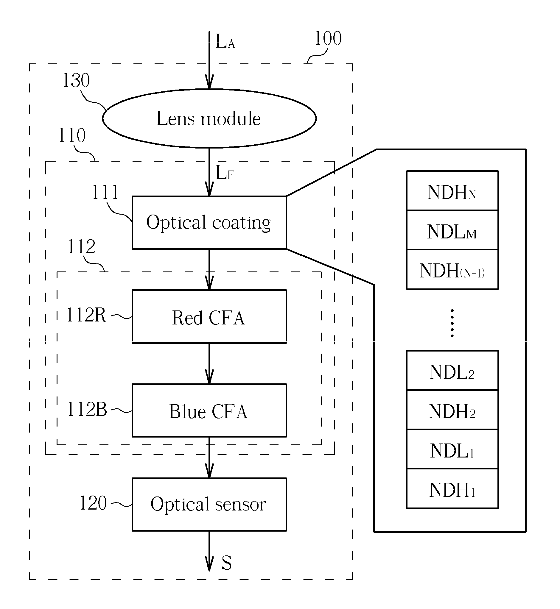
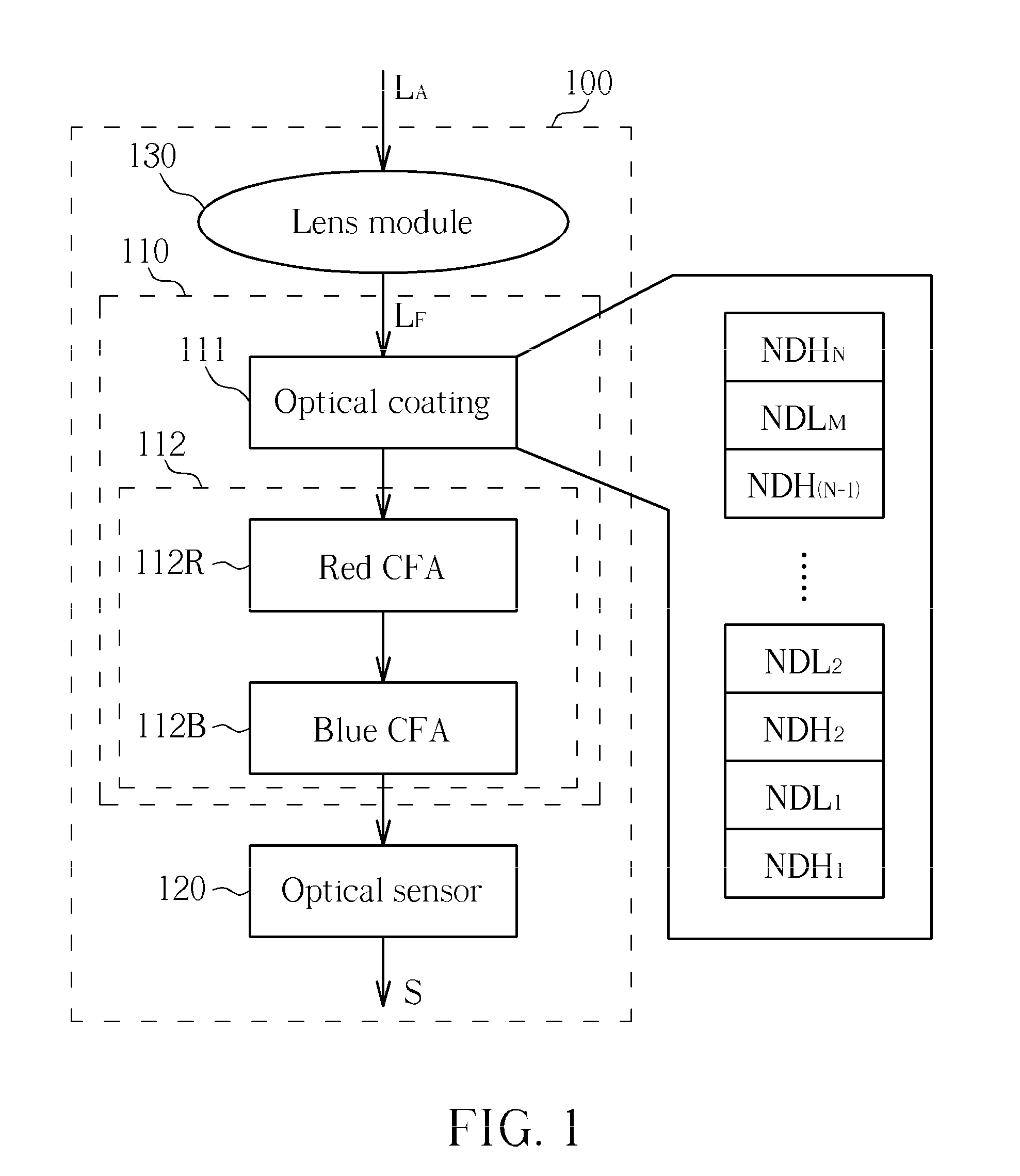
[0028]Please refer to FIG. 1. FIG. 1 is a diagram illustrating an IR sensing device 100 according to the present invention. The IR sensing device 100 comprises an IR pass filter 110, an optical sensor 120, and a lens module 130. An optical path exists on the IR sensing device 100 for allowing an ambient light LA to enter the optical sensor 120.

[0029]The lens module 130, disposed on the optical path, provides a focused light LF out of an ambient light LA from a scene. That is, the lens module 130 focuses the ambient light LA to be the focused light LF. The optical sensor 120, disposed on the optical path, may comprise a photo diode, where photons absorbed by the photo diode generate an electrical signal S, either a voltage or current signal, indicative of the number of photons absorbed by the photo diode.

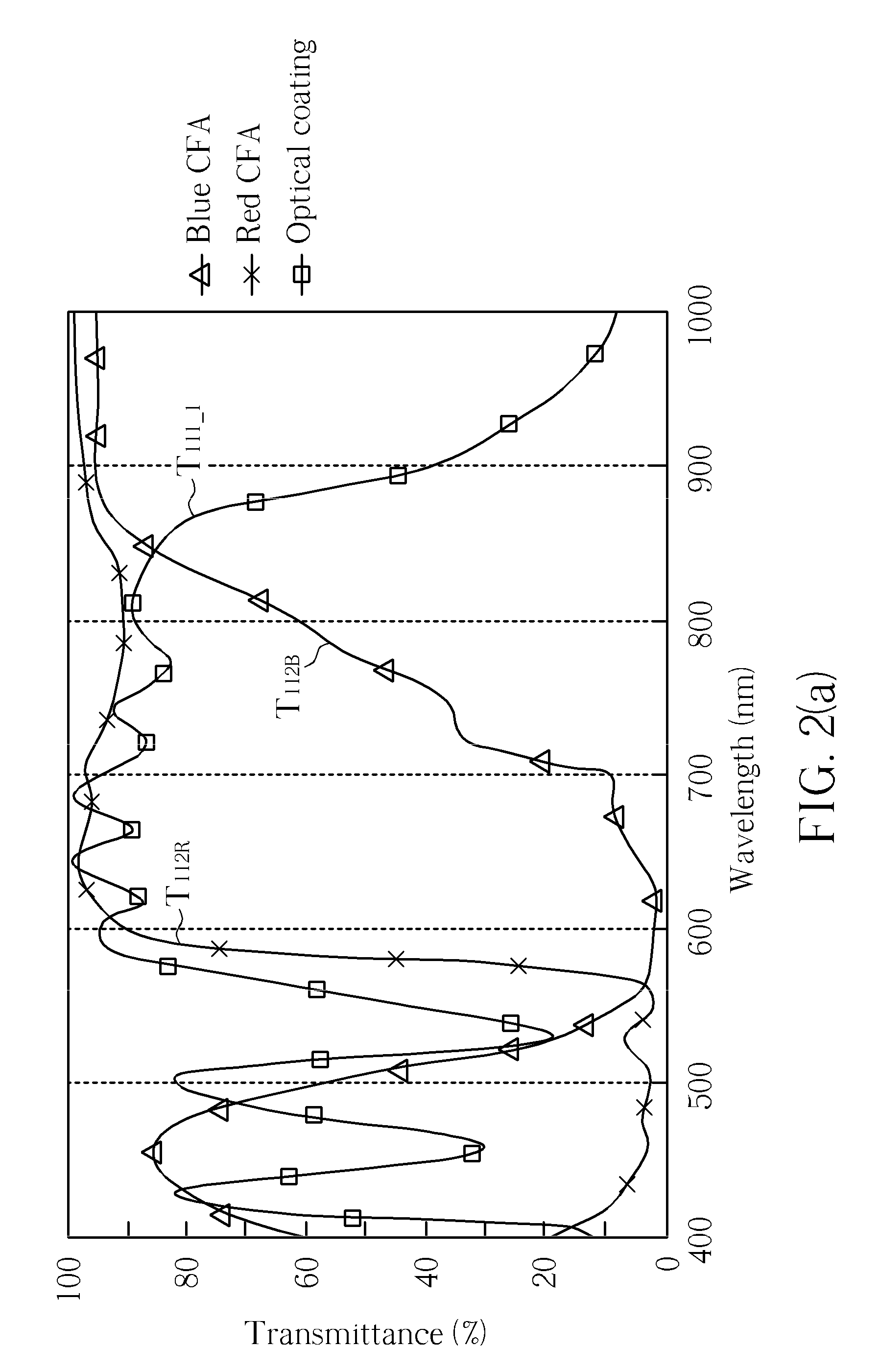
[0030]The IR pass filter 110, disposed on the optical path, comprises an optical coating 111, and a CFA module 112. The CFA module 112 comprises a red and a blue CFAs 112R and 112B. ...

second embodiment

[0035]Please refer to FIG. 4. FIG. 4 is a diagram illustrating an IR sensing device 400 according to the present invention. The IR light sensing device 400 comprises an IR pass filter 410, an optical sensor 120, and a lens module 130. The IR pass filter 410 comprises an optical coating 111, and a CFA module 412. The CFA module 412 comprises a red CFA 112R, a blue CFA 112B, and a green CFA 112G. The green CFA 112G mainly blocks light with the wavelength around 400 nm to 475 nm, and the wavelength around 600 nm to 780 nm.

[0036]Please refer to FIG. 5. FIG. 5(a) is a diagram illustrating the transmittance spectrums T111—1, T112R, T112B, and T112G respectively of the optical coating 111 with the first setting, the red CFA 112R, the blue CFA 112B, and the green CFA 112G of the present invention. FIG. 5(b) is a diagram illustrating the resulting transmittance spectrum T410—1 of the IR pass filter 410 of the present invention from FIG. 5(a). In the sensitive range for the optical sensor 120...

third embodiment

[0038]Please refer to FIG. 7. FIG. 7 is a diagram illustrating the structure view of the IR sensing device 700 according to the present invention. The IR sensing device 700 may be realized with the IR sensing devices 100 or 400. As shown in FIG. 7, the CFA module 712, the optical coating 711, and the optical sensor 720 can be integrated as an Integrated Chip (IC). More particularly, in the IC, the CFA module 712 is coated on the optical sensor 720, and the optical coating 711 is coated on the CFA module 712. The lens module 730 is disposed on the upside of the optical coating 711 of the IC.


PUM


Abstract

An Infrared Radiation (IR) sensing device comprises a lens module, an IR pass filter, and an optical sensor. The lens module is utilized for focusing light. The IR pass filter comprises an optical coating, and a Color Filter Array (CFA) module. The optical coating is utilized for blocking light with wavelength around a predetermined range. The CFA module is utilized for blocking light with wavelength around 400 nm to 780 nm. The optical sensor for absorbing photons of light after being blocked by the IR pass filter on the optical path and accordingly generating an electrical signal. With the help of the CFAs, the range of the wavelength that the optical coating has to block becomes smaller, which greatly reduces the required number of layers of the optical coating.

Description

CROSS REFERENCE TO RELATED APPLICATIONS[0001]This application claims the benefit of U.S. Provisional Application No. 61 / 161,077, filed on Mar. 18, 2009 and entitled “Infrared pass filter” the contents of which are incorporated herein.BACKGROUND OF THE INVENTION[0002]1. Field of the Invention[0003]The present invention relates to an Infrared Radiation (IR) sensing device, and more particularly, to an IR sensing device by means of overlaying one or more Color Filter Arrays (CFA) along with the optical coating for passing IR and filtering non-IR out.[0004]2. Description of the Prior Art[0005]IR sensing devices based on silicon technology typically require the use of a non-infrared blocking element somewhere in the optical chain for only responding IR. The purpose of this element is to prevent non-infrared radiation (IR) or light (typically considered to be light with a wavelength longer than 780 nm) from entering the optical sensors of the optical sensing devices. Silicon-based optical...

Claims


Application Information

Patent Timeline
Patent Type & Authority Patents(United States)
IPC IPC(8): G01J5/02G01J3/50
CPCH01L27/14618H01L27/14621H01L27/14625H01L31/0203H01L31/02162H04N5/33H01L2924/0002H01L31/02325H04N23/57H01L2924/00
Inventor CHEN, HUI-HSUAN
Owner PIXART IMAGING INC
Why Eureka
Try Eureka