Liquid crystal display device

a liquid crystal display and display panel technology, applied in non-linear optics, instruments, optics, etc., can solve the problems of short h, damage to the glass substrate that forms the liquid crystal display panel, inefficient positioning process, etc., and achieve the effect of thin liquid crystal display and convenient positioning

Active Publication Date: 2013-05-21
JAPAN DISPLAY INC +1
View PDF15 Cites 6 Cited by
  • Summary
  • Abstract
  • Description
  • Claims
  • Application Information

AI Technical Summary

Benefits of technology

[0015]An object of the present invention is to solve the above described problem and provide a thin liquid crystal display device where it is easy to position the flexible printed circuit on which light emitting diodes are mounted.
[0018]According to the present invention, through holes for positioning are created in both the flexible printed circuit and the mold frame, and a pin on the assembly jig is inserted into these through holes when the liquid crystal display device is assembled. Thus, the flexible printed circuit on which light emitting diodes are mounted can be easily positioned, and after assembly, the assembly jig is removed and the pin that protrudes from the rear surface of the liquid crystal display device is removed, and therefore it is possible to provide a thin liquid crystal display device.

Problems solved by technology

Though it is necessary to make the length h of the boss pin 3 as short as possible, particularly in order to make the liquid crystal display device thinner, the process for positioning the portion 2 becomes inefficient when h is short.
In addition, when stress is applied to a boss pin 3 during or after the incorporation of the liquid crystal display device into the main body, such as of a portable phone, stress is applied to the liquid crystal display panel held in the mold frame MFR as well, and there is a risk of a glass substrate that forms the liquid crystal display panel being damaged.

Method used


Image

  • Liquid crystal display device
  • Liquid crystal display device
  • Liquid crystal display device

Examples


Embodiment Construction

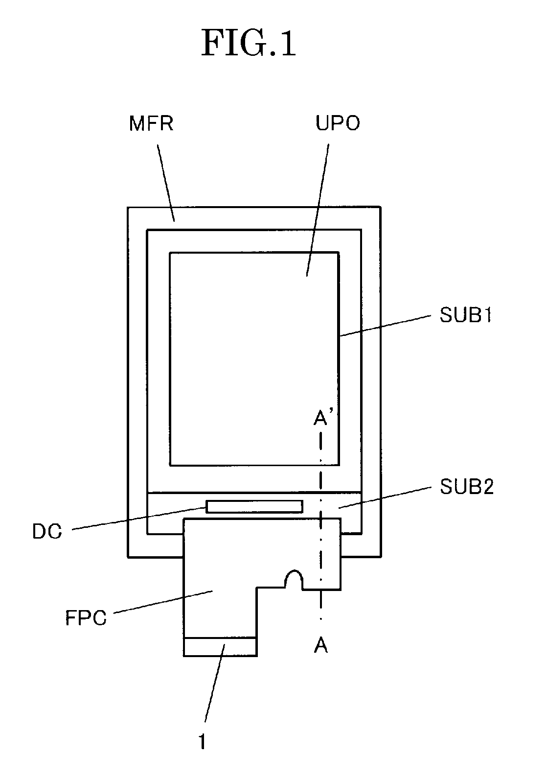
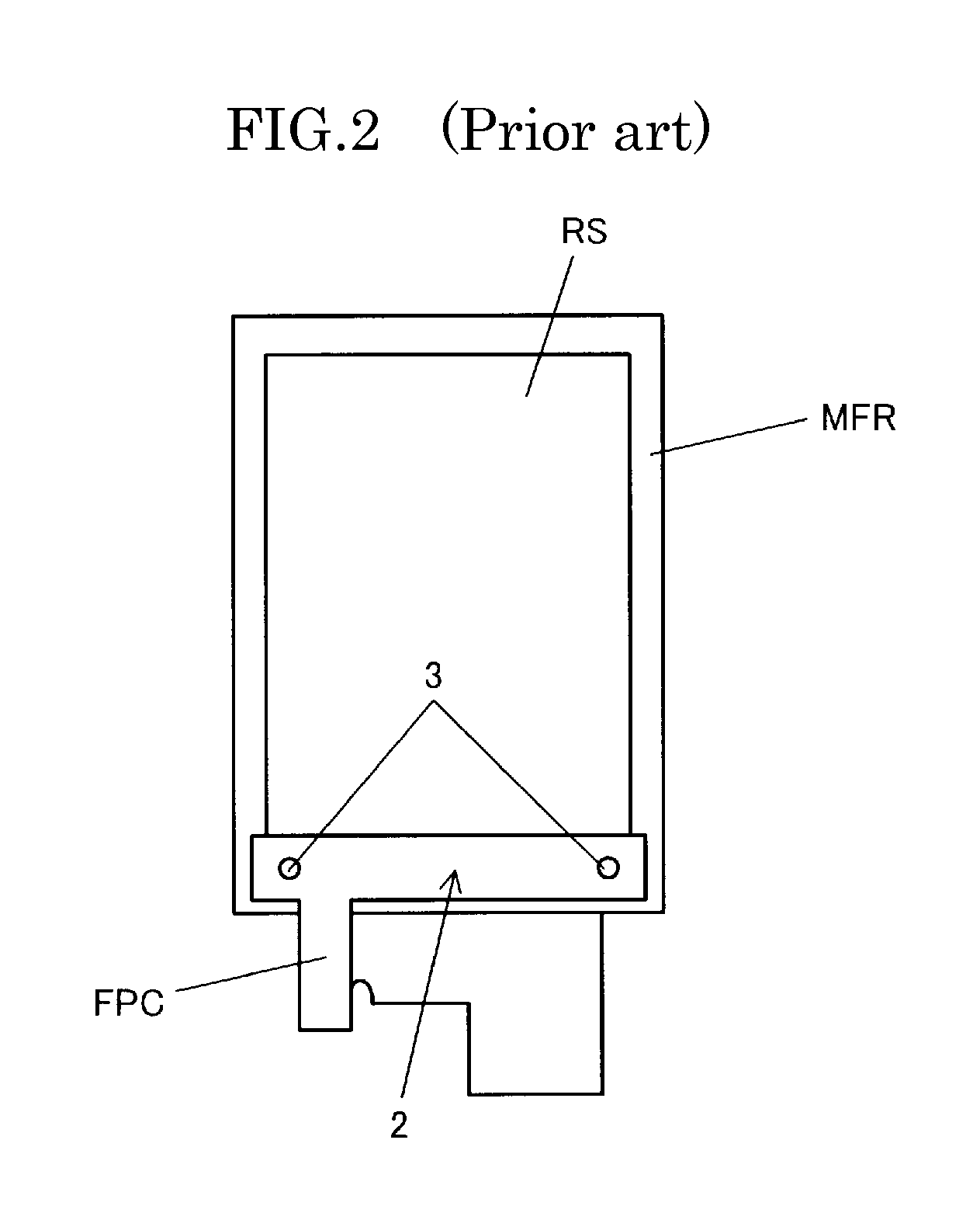
[0035]The liquid crystal display device according to the present invention is the same as the one shown in FIGS. 1, 3, 4 and 6, and therefore the descriptions thereof are omitted. The structure according to the present invention is described in detail below.

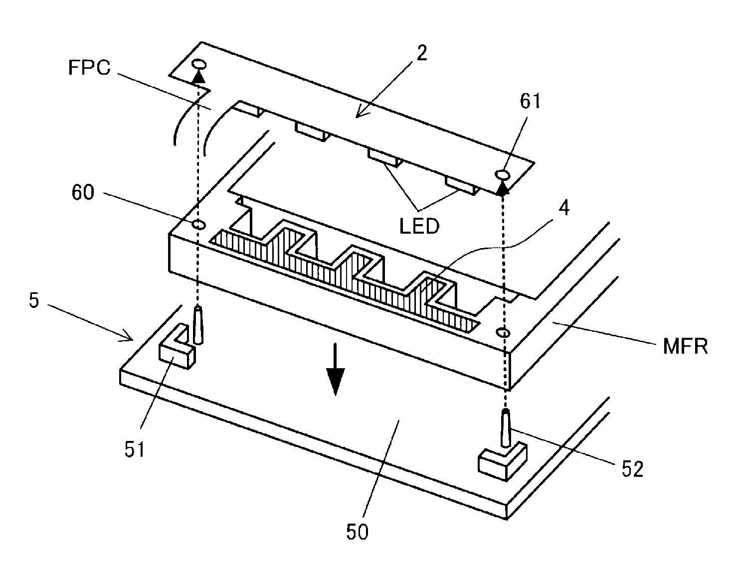
[0036]As shown in FIG. 10, the liquid crystal display device according to the present invention has a liquid crystal display panel (not shown) and a flexible printed circuit (FPC) that is connected to the liquid crystal display panel and supplies power for driving display pixels, and is characterized in that light emitting diodes (LED) are mounted on a portion of the flexible printed circuit, a mold frame (MFR) is provided to contain the light emitting diodes, and through holes (61, 60) for positioning are created in both the flexible printed circuit and the mold frame.

[0037]As shown in FIG. 10, an assembly jig 5 where means 51 for positioning the mold frame and pins 52 are provided in predetermined locations of a plate 50. The p...


PUM

PropertyMeasurementUnit
flexibleaaaaaaaaaa
thicknessaaaaaaaaaa
lengthaaaaaaaaaa

Abstract

The liquid crystal display device according to the present invention is a thin liquid crystal display device where it is easy to position the flexible printed circuit on which light emitting diodes are mounted. In the liquid crystal display device having a liquid crystal display panel and a flexible printed circuit (FPC) that is connected to the liquid crystal display panel and supplies power for driving display pixels, light emitting diodes (LED) are mounted on a portion of the flexible printed circuit, a mold frame MFR is provided to contain the light emitting diodes, and through holes (60, 61) for positioning are created in both the flexible printed circuit and the mold frame.

Description

CROSS-REFERENCE TO RELATED APPLICATION[0001]The present application claims priority over Japanese application JP2010-078924 filed on Mar. 30, 2010, the contents of which are hereby incorporated into this application by reference.BACKGROUND OF THE INVENTION[0002](1) Field of the Invention[0003]The present invention relates to a liquid crystal display device, and in particular to a liquid crystal display device where positioning of a flexible printed circuit connected to the liquid crystal display panel is improved.[0004](2) Description of the Related Art[0005]Liquid crystal display modules (liquid crystal display devices) are used as the display device of various portable information apparatuses, such as portable phones, portable information terminals (PDA's), digital cameras and multimedia players.[0006]The demand is high for reducing the thickness and narrowing the frame of these liquid crystal display modules, such as portable phones. Therefore, as shown in JP2010-276808A, in the ...

Claims


Application Information

Patent Timeline
Patent Type & Authority Patents(United States)
IPC IPC(8): G02F1/1345
CPCG02F1/133615G02F1/13452
Inventor OOHIRA, EIJI
Owner JAPAN DISPLAY INC
Why Eureka
Try Eureka