Stackable variable height via package and method

a variable height and stacking technology, applied in the field of electronic components, can solve the problems of fundamental restrictions on minimizing the pitch of solder balls

Active Publication Date: 2013-06-25
AMKOR TECH SINGAPORE HLDG PTE LTD
View PDF176 Cites 63 Cited by
  • Summary
  • Abstract
  • Description
  • Claims
  • Application Information

AI Technical Summary

Benefits of technology

[0009]Forming the stackable variable height via package with variable height vias readily accommodate stacking of additional packages having different types of terminals, e.g., LGA and BGA type packages, as well as variable degrees of warpage on the stackable variable height via package. Further, the vias are formed with a minimum pitch.

Problems solved by technology

Thus, forming the solder balls with a height greater than the height of the encapsulant places fundamental restrictions on minimizing the pitch of the solder balls.

Method used


Image

  • Stackable variable height via package and method
  • Stackable variable height via package and method
  • Stackable variable height via package and method

Examples


Embodiment Construction

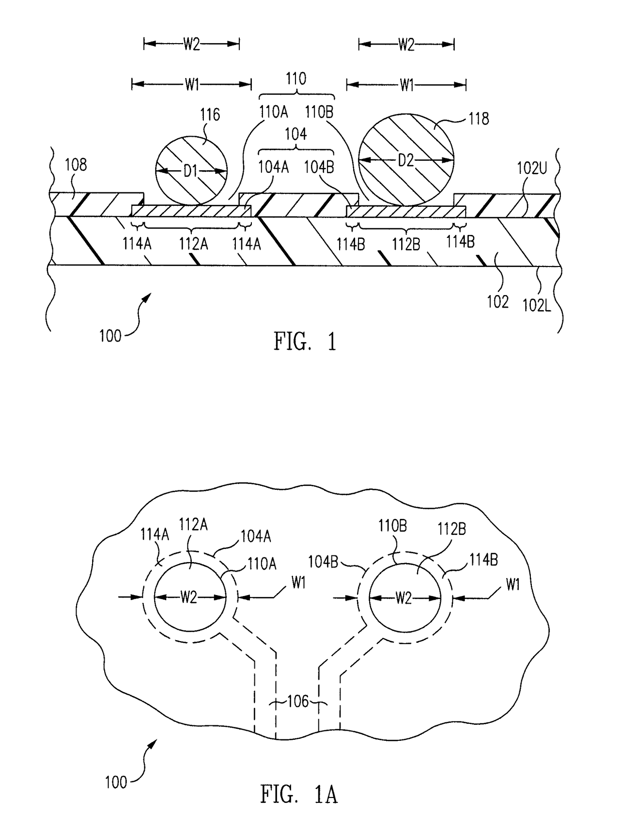
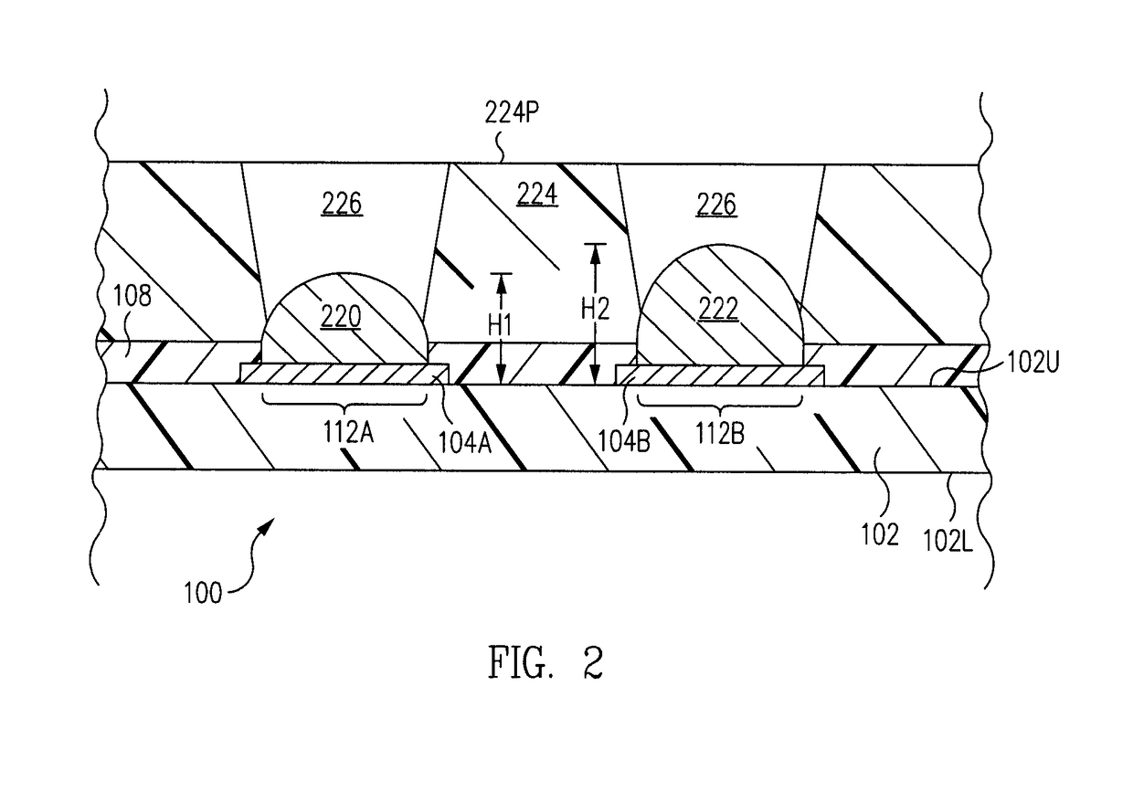
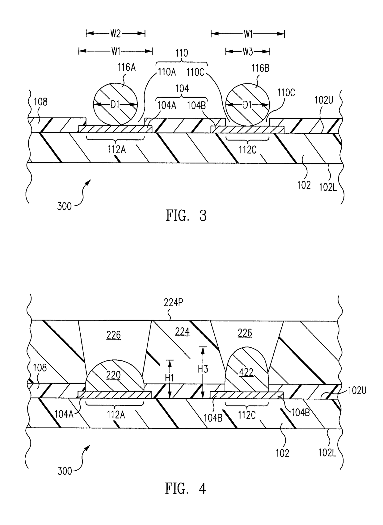
[0035]As an overview and in accordance with one embodiment, referring to FIGS. 2 and 14 together, a stackable variable height via package 1300 includes a substrate 102 having an upper surface 102U including terminals 104 formed thereon. Terminals 104 include a first terminal 104A and a second terminal 104B. Vias 220, 222 are on terminals 104, vias 220, 222 including a first via 220 on first terminal 104A and a second via 222 on second terminal 104B. Via 220 has a height H1 from upper surface 102U of substrate 102 less than a height H2 of via 222 from upper surface 102U of substrate 102. Variable height via package 1300 further includes a package body 224 and via apertures 226 in package body 224 to expose vias 220, 222.

[0036]Forming stackable variable height via package 1300 with variable height vias 220, 222 readily accommodate stacking of additional packages having different types of terminals (for example, see LGA and BGA type packages 1554, 1560A, 1560B of FIG. 15), as well as v...


PUM

PropertyMeasurementUnit
heightaaaaaaaaaa
conductiveaaaaaaaaaa
surface areaaaaaaaaaaa

Abstract

A stackable variable height via package includes a substrate having a first surface and terminals thereon. The terminals include a first terminal and a second terminal. Vias are on the terminals, the vias including a first via on the first terminal and a second via on the second terminal. The first via has a height from the first surface of the substrate less than a height of the second via from the first surface of the substrate. The package further includes a package body and via apertures in the package body to expose the vias. Forming the stackable variable height via package with variable height vias readily accommodate stacking of additional packages having different types of terminals, e.g., LGA and BGA type packages, as well as variable degrees of warpage on the stackable variable height via package. Further, the vias are formed with a minimum pitch.

Description

BACKGROUND OF THE INVENTION[0001]1. Field of the Invention[0002]The present application relates to the field of electronics, and more particularly, to methods of forming electronic component packages and related structures.[0003]2. Description of the Related Art[0004]To form an electronic component package, an electronic component is mounted to a substrate. The substrate includes traces on the same surface of the substrate to which the electronic component is mounted. Bond wires are formed to electrically connect bond pads of the electronic component to the traces.[0005]To protect the electronic component as well as the bond wires, the electronic component and bond wires are covered in an encapsulant. The traces extend from under the encapsulant to an exposed area of the surface of the substrate outside of the periphery of the encapsulant, i.e., not covered by the encapsulant. The traces include terminals on the exposed area of the substrate outside of and around the encapsulant.[00...

Claims


Application Information

Patent Timeline
Patent Type & Authority Patents(United States)
IPC IPC(8): H05K1/16
CPCH01L23/3128H01L23/49811H01L25/105H01L2924/3511H01L2224/73204H01L2224/48091H01L2225/06568H01L2924/15331H01L2924/15311H01L2924/15192H01L2225/1058H01L2225/1023H01L2225/0651H01L23/49816H01L2225/1076H01L2224/16225H01L2224/32145H01L2224/32225H01L2224/48227H01L2224/73265H01L2924/00014H01L2924/00012H01L2924/00H01L24/73H01L2924/1815Y10T29/49002H05K3/42
Inventor YOSHIDA, AKITODREIZA, MAHMOUD
Owner AMKOR TECH SINGAPORE HLDG PTE LTD
Why Eureka
Try Eureka