Light emitting device and display panel

a technology of light emitting device and display panel, which is applied in the direction of static indicating device, discharge tube luminescnet screen, instruments, etc., can solve the problem of insufficient light emission amount, and achieve the effect of increasing the amount of light emission and reducing the total reflection

Active Publication Date: 2013-07-23
AU OPTRONICS CORP
View PDF6 Cites 0 Cited by
  • Summary
  • Abstract
  • Description
  • Claims
  • Application Information

AI Technical Summary

Benefits of technology

[0008]The invention is directed to a light emitting device capable of increasing light emission amount of a device.
[0009]The invention is further directed to a light emitting device capable of reducing total reflection of light in a device.
[0024]Based on the above, the patterned light-scattering layer is disposed on the substrate, and the electroluminescent device is disposed on the patterned light-scattering layer according to this invention, such that the light emitted from the electroluminescent device can be scattered when the light passes through the patterned light-scattering layer. The scattered light can enter the substrate at different angles, so as to reduce total reflection and increase the amount of light emission.

Problems solved by technology

Thereby, total reflection occurs at an interface between the transparent conductive layer and a substrate or at an interface between the substrate and the air, and the light emission amount is insufficient because the light is not able to be transmitted out.

Method used


Image

  • Light emitting device and display panel
  • Light emitting device and display panel
  • Light emitting device and display panel

Examples


Embodiment Construction

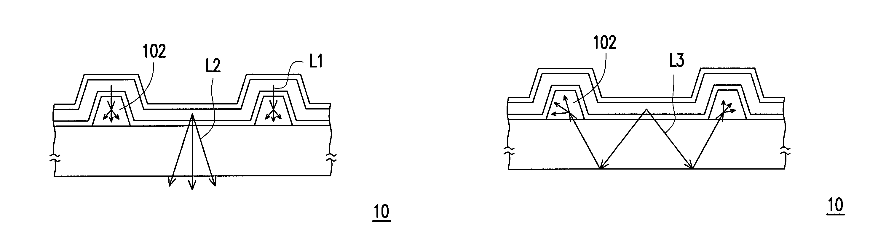
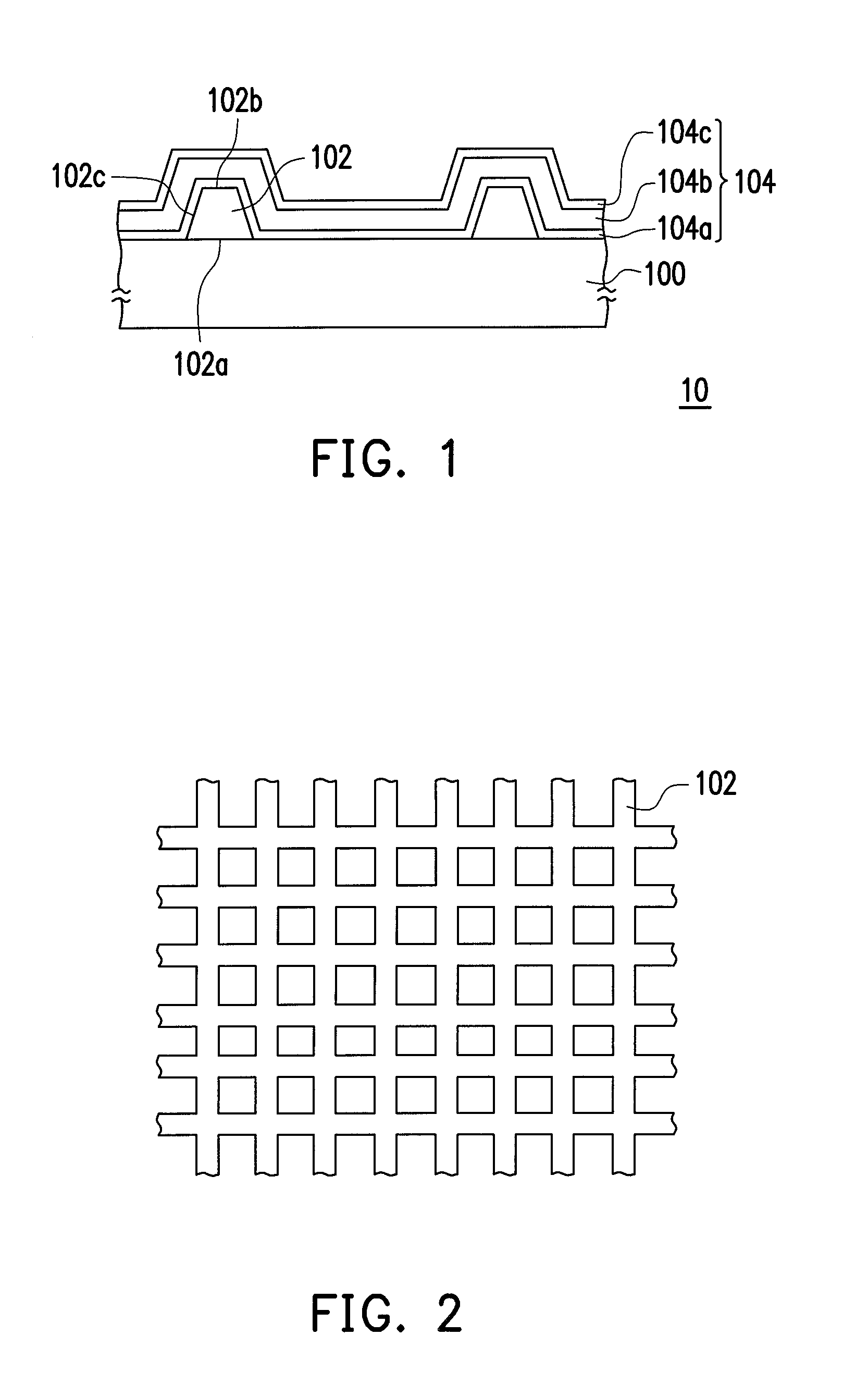
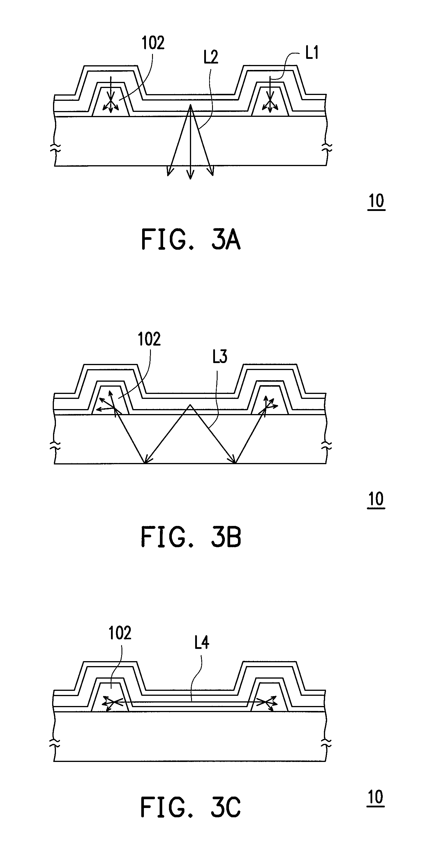
[0031]FIG. 1 is a schematic cross-sectional view illustrating a light emitting device according to an embodiment of the invention. As shown in FIG. 1, a light emitting device 10 of this embodiment includes a substrate 100, a patterned light-scattering layer 102, and an electroluminescent device 104. The electroluminescent device 104 is organic or inorganic electroluminescent device, for example. The substrate 100 is a transparent substrate (e.g. a glass substrate). The patterned light-scattering layer 102 is disposed on a portion of the substrate 100, for instance. The patterned light-scattering layer 102 has a bottom surface 102a in contact with the substrate 100, a top surface 102b opposite to the bottom surface 102a, and sidewalls 102c connecting the bottom surface 102a and the top surface 102b. An included angle formed between each of the sidewalls 102c and the bottom surface 102a is an acute angle ranging from about 5° to about 65°, for example. In addition, an area of the top ...


PUM


Abstract

A light emitting device includes a substrate, a patterned light-scattering layer, and an electroluminescent device. The patterned light-scattering layer is disposed on a portion of the substrate. The patterned light-scattering layer has a bottom surface in contact with the substrate, a top surface opposite to the bottom surface, and a plurality of sidewalls connecting the bottom surface and the top surface. The electroluminescent device is at least disposed on the sidewalls.

Description

CROSS-REFERENCE TO RELATED APPLICATION[0001]This application claims the priority benefit of Taiwan application serial no. 99112680, filed on Apr. 22, 2009. The entirety of the above-mentioned patent application is hereby incorporated by reference herein and made a part of this specification.BACKGROUND OF THE INVENTION[0002]1. Field of the Invention[0003]The invention relates to a light emitting device and a display panel. More particularly, the invention relates to a light emitting device and a display panel which can improve the light emission amount of a device.[0004]2. Description of Related Art[0005]An organic electroluminescent device is a semiconductor device capable of efficiently converting electrical energy into optical energy, and the organic electroluminescent device often serves as a light emitting device of indicator light, a display panel, and an optical pickup head. Since the organic electroluminescent device is characterized by the absence of viewing-angle dependence...

Claims


Application Information

Patent Timeline
Patent Type & Authority Patents(United States)
IPC IPC(8): H01L51/00
CPCH01L51/5268H10K50/854
Inventor LIN, CHUN-LIANGFANG, CHUN-HSIANGLIN, CHEN-CHILIU, CHUNG-WEI
Owner AU OPTRONICS CORP
Why Eureka
Try Eureka