
Sensitivity and static timing analysis for integrated circuit designs using a multi-CCC current source model

Inactive Publication Date: 2013-08-20
CADENCE DESIGN SYST INC
View PDF15 Cites 16 Cited by
  • Summary
  • Abstract
  • Description
  • Claims
  • Application Information

AI Technical Summary

Benefits of technology

The invention has various benefits and options for use. The technical effects of the invention are outlined below.

Problems solved by technology

Additionally with the smaller geometries there may be a number of unknown effects to electronic signal propagation that may be considered, which may not have been as severe with more relaxed process technology nodes.

Method used


Image

  • Sensitivity and static timing analysis for integrated circuit designs using a multi-CCC current source model
  • Sensitivity and static timing analysis for integrated circuit designs using a multi-CCC current source model
  • Sensitivity and static timing analysis for integrated circuit designs using a multi-CCC current source model

Examples


Embodiment Construction

[0038]In the following detailed description of the embodiments of the invention, numerous specific details are set forth in order to provide a thorough understanding. However, it will be obvious to one skilled in the art that the embodiments of the invention may be practiced without these specific details. In other instances well known methods, procedures, components, and circuits have not been described in detail so as not to unnecessarily obscure aspects of the embodiments of the invention.

Introduction

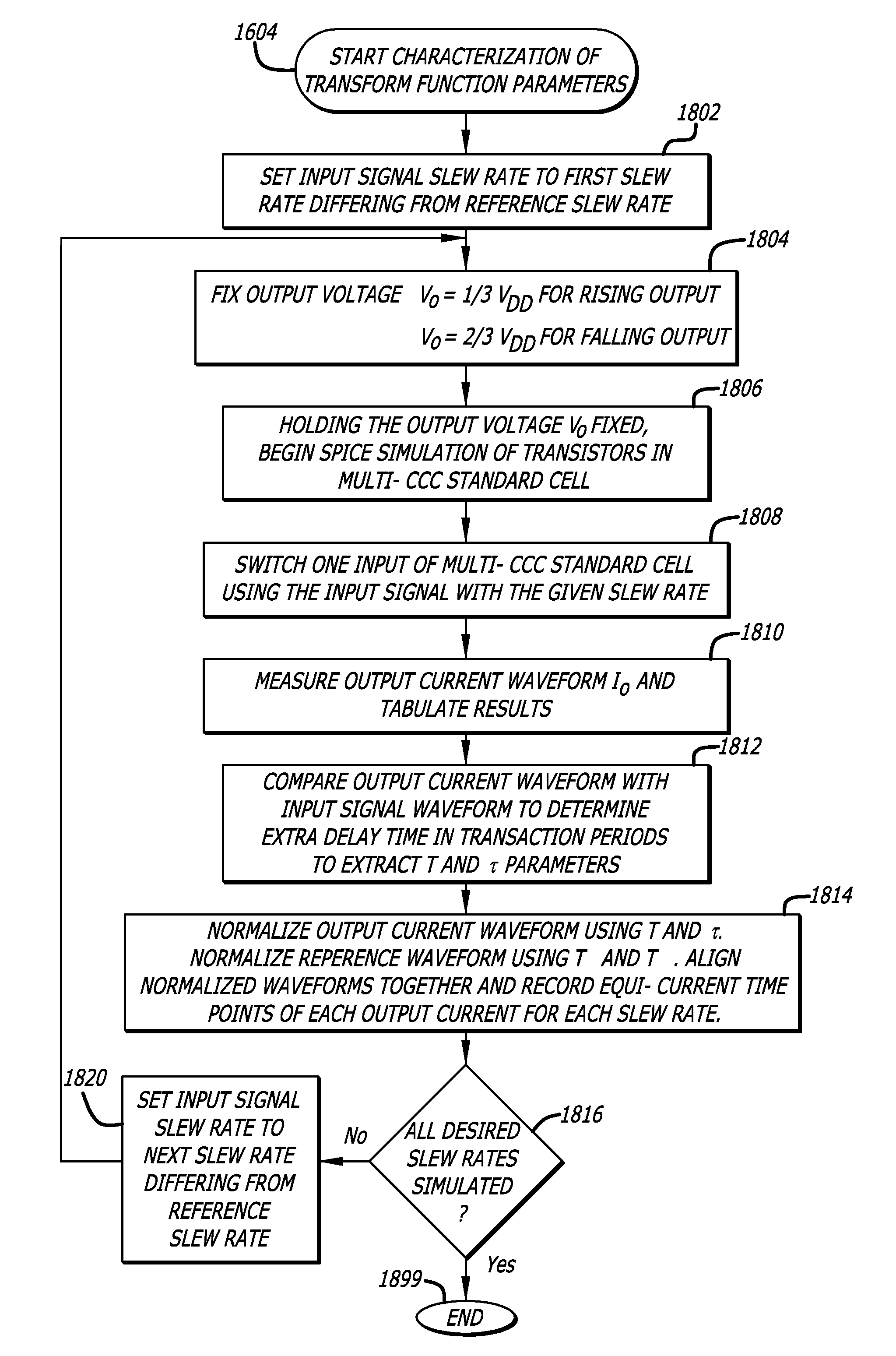
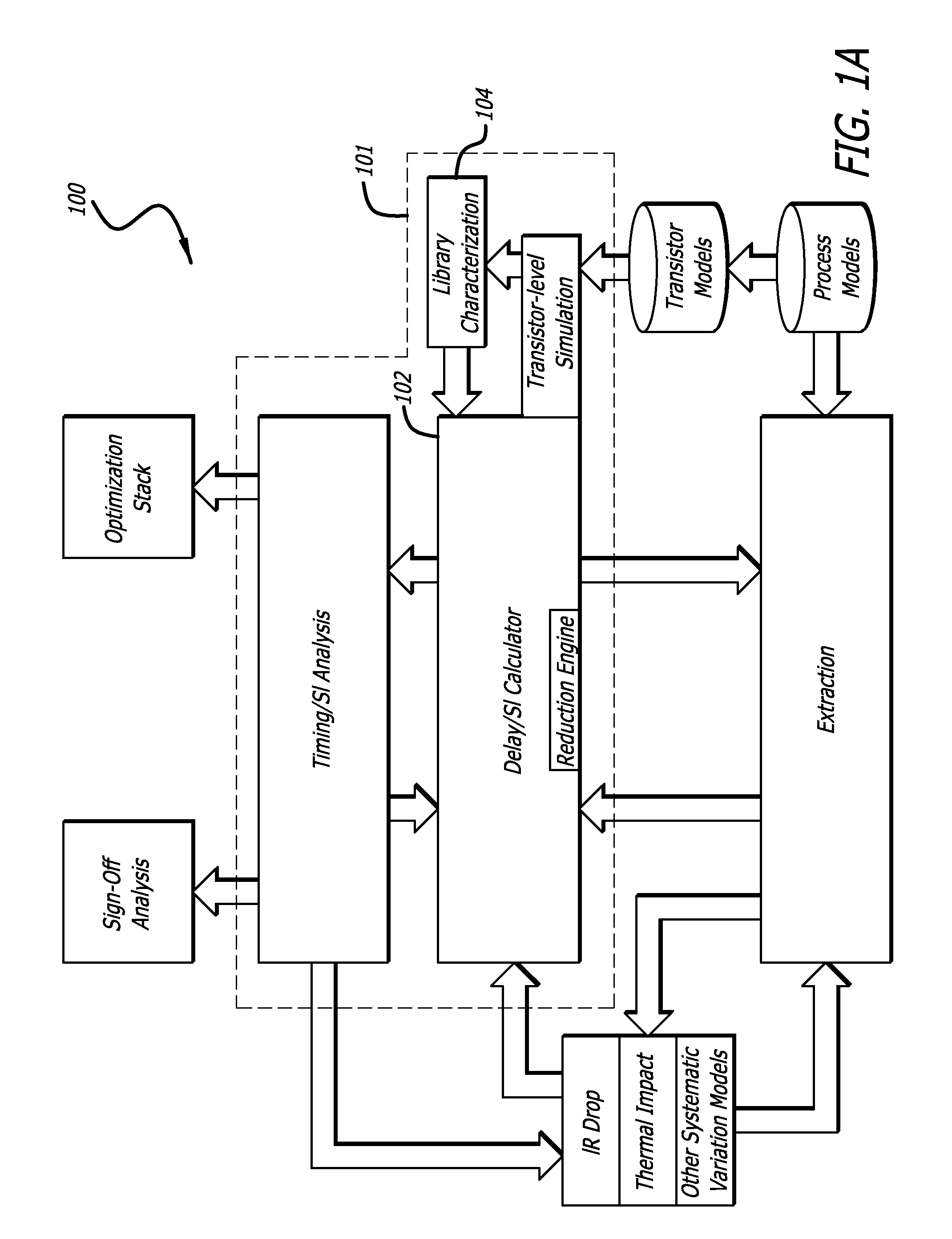
[0039]FIG. 1A illustrates an exemplary integrated circuit design flow 100 employing embodiments of the invention. Digital performance analysis software tools, such as Static Timing Analysis (STA) software tools and Signal Integrity (SI) Analysis software tools 101, are used to estimate the performance of an integrated circuit chip. As shown in FIG. 1A, these software tools may internally employ different levels of abstraction, a graph level abstraction, a net level abstraction, and a...


PUM


Abstract

In one embodiment of the invention, a multi-CCC current source model is disclosed to perform statistical timing analysis of an integrated circuit design. The multi-CCC current source model includes a voltage waveform transfer function, a voltage dependent current source, and an output capacitor. The voltage waveform transfer function receives an input voltage waveform and transforms it into an intermediate voltage waveform. The voltage dependent current source generates an output current in response to the intermediate voltage waveform. The output capacitor is coupled in parallel to the voltage dependent current source to generate an output voltage waveform for computation of a timing delay.

Description

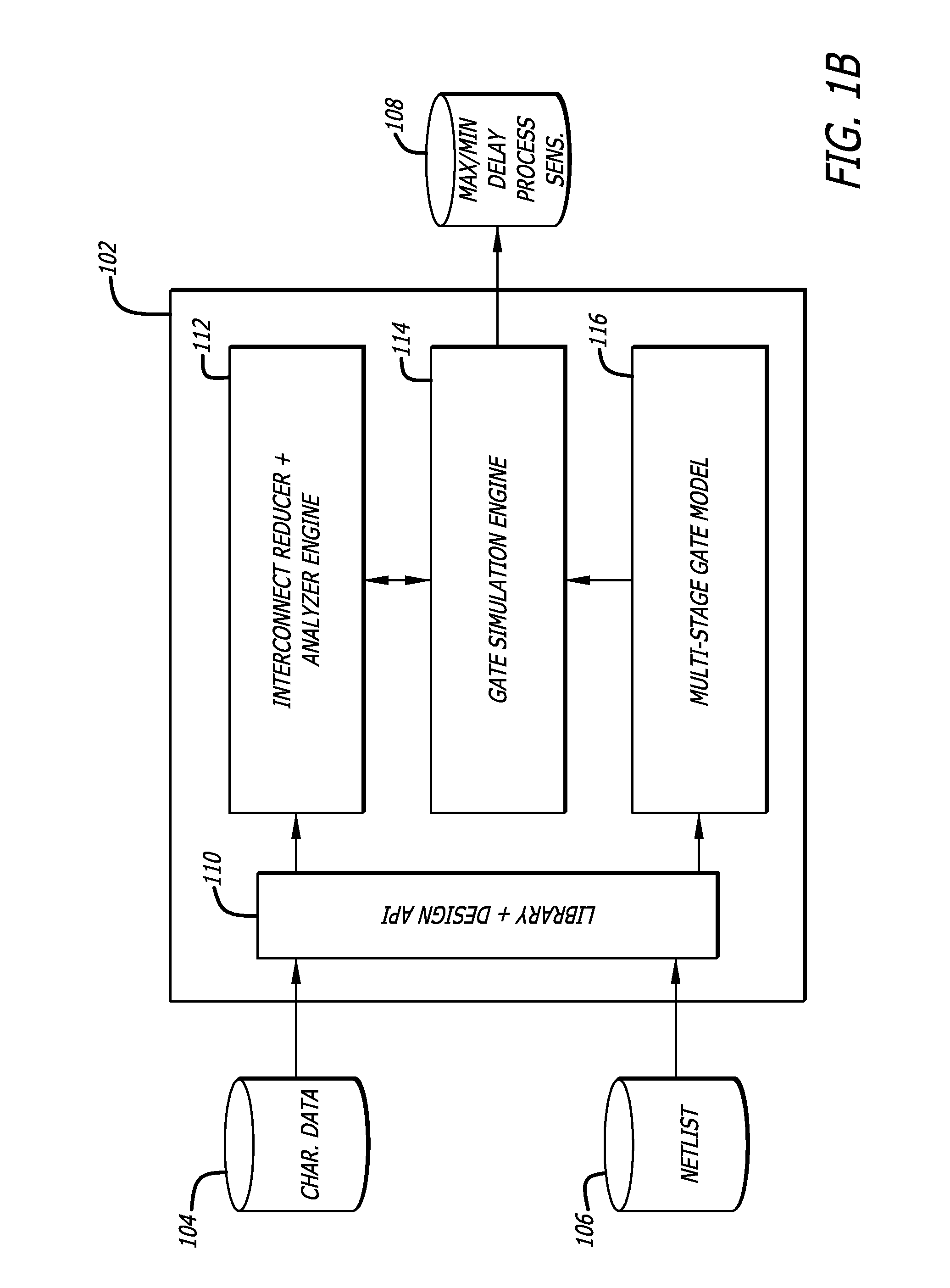
FIELD[0001]The embodiments of the invention relate generally to integrated circuit design software tools, such as static timing analysis software tools and signal integrity analysis software tools for designing integrated circuits.BACKGROUND[0002]Electronic computer aided design (ECAD) software tools for static timing analysis (STA) may be used to estimate timing delays in an electronic circuit such as that found in an integrated circuit. However as process technology improves so that smaller transistor channels of 65 nano-meters (nm) and 45 nm become available, there is an increased need for even more accurate timing analysis. Additionally with the smaller geometries there may be a number of unknown effects to electronic signal propagation that may be considered, which may not have been as severe with more relaxed process technology nodes.BRIEF SUMMARY[0003]The embodiments of the invention are summarized by the claims that follow below.BRIEF DESCRIPTIONS OF THE DRAWINGS[0004]FIG. 1...

Claims


Application Information

Patent Timeline
Patent Type & Authority Patents(United States)
IPC IPC(8): G06F17/50
CPCG06F17/5036G06F17/5081G06F2217/84G06F2119/12G06F30/367G06F30/398
Inventor KARIAT, VINODKELLER, IGORPHILLIPS, JOEL R.TAM, KING HO
Owner CADENCE DESIGN SYST INC
Learn More