Dual-side interconnected CMOS for stacked integrated circuits

a technology of integrated circuits and stacked circuits, applied in the field of integrated circuits, can solve the problems of limiting the height of stacked circuits, and ultra-thin cellular phones may not support stacked circuits having multiple dies

Active Publication Date: 2013-09-03
QUALCOMM INC
View PDF22 Cites 178 Cited by
  • Summary
  • Abstract
  • Description
  • Claims
  • Application Information

AI Technical Summary

Problems solved by technology

However, in some applications the height of the stacked IC is restricted.
For example, ultra-thin cellular phones may not support stacked ICs having multiple dies.

Method used


Image

  • Dual-side interconnected CMOS for stacked integrated circuits
  • Dual-side interconnected CMOS for stacked integrated circuits
  • Dual-side interconnected CMOS for stacked integrated circuits

Examples


Embodiment Construction

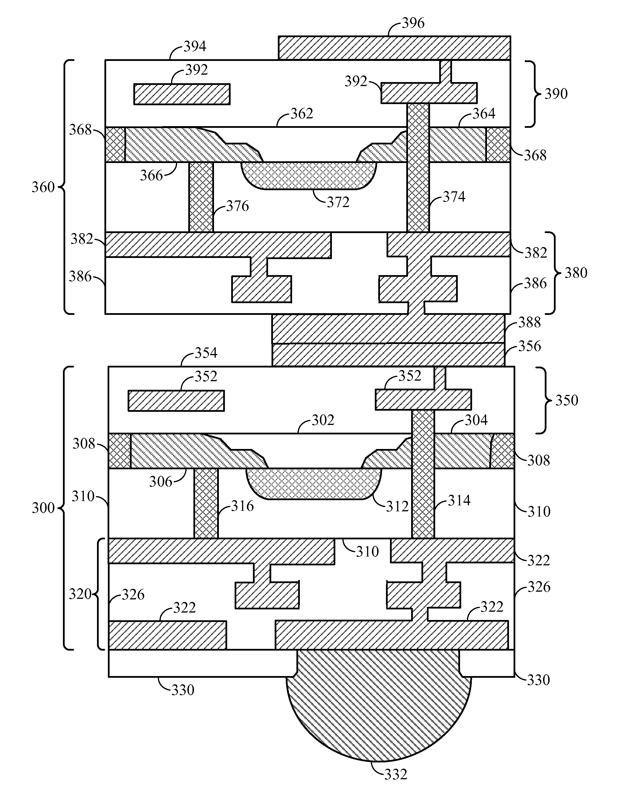
[0015]Reducing the height of stacked integrated circuits (ICs) may be accomplished with dual-side interconnected integrated circuits. According to one embodiment, a combination of regular contacts and extended contacts are etched in an integrated circuit. The regular contacts allow coupling to the front side of the integrated circuit, and the extended contacts allow coupling to the front side and back side of the integrated circuit. Dual-side integrated circuits allow construction of ultra-thin stacked integrated circuits. Additionally, very high density tier-to-tier connections in the stacked IC are made possible.

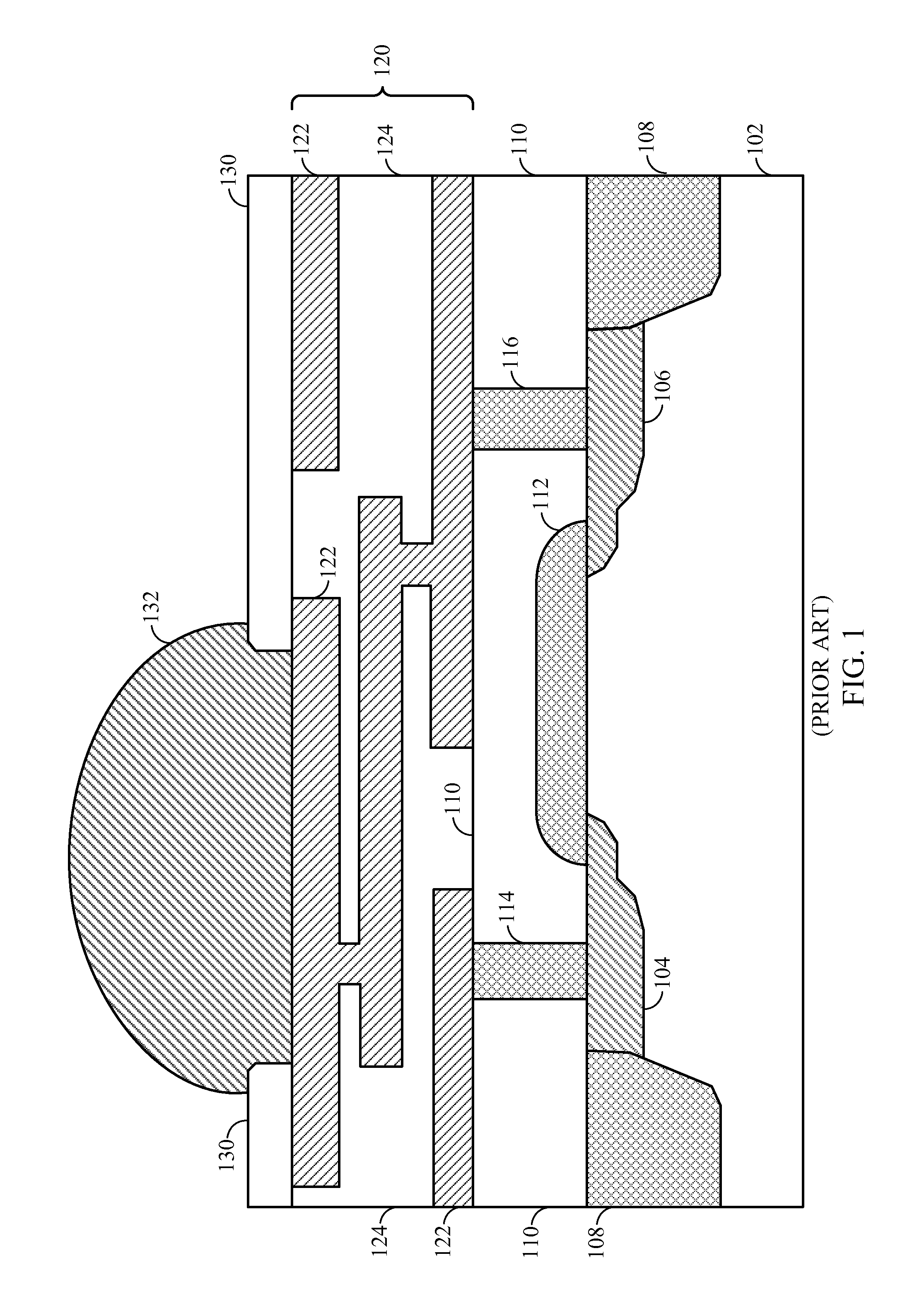
[0016]FIG. 1 is a cross-sectional view illustrating a conventional semiconductor die. A bulk semiconductor layer 102 such as silicon includes a source region 104 and a drain region 106. Trench isolation regions 108 isolate the regions 104, 106 from other regions in the bulk semiconductor layer 102. A gate structure 112 is formed between the regions 104, 106 and on the bulk...


PUM


Abstract

A stacked integrated circuit (IC) may be manufactured with a second tier wafer bonded to a double-sided first tier wafer. The double-sided first tier wafer includes back-end-of-line (BEOL) layers on a front and a back side of the wafer. Extended contacts within the first tier wafer connect the front side and the back side BEOL layers. The extended contact extends through a junction of the first tier wafer. The second tier wafer couples to the front side of the first tier wafer through the extended contacts. Additional contacts couple devices within the first tier wafer to the front side BEOL layers. When double-sided wafers are used in stacked ICs, the height of the stacked ICs may be reduced. The stacked ICs may include wafers of identical functions or wafers of different functions.

Description

TECHNICAL FIELD[0001]The present disclosure generally relates to integrated circuits. More specifically, the present disclosure relates to packaging integrated circuits.BACKGROUND[0002]Stacked ICs increase device functionality and decrease occupied area by stacking dies vertically. In stacked ICs, a second die is stacked on a first die allowing construction to expand into three dimensions (3D). Stacked ICs allow products with a greater number of components to fit in small form factors. Component density of a semiconductor die is the number of components in the die divided by the die area. For example, stacking a die on an identical die results in approximately double the number of components in the same area to double component density. When a second die is stacked on a first die, the two dies share the same packaging and communicate to external devices through the packaging.[0003]Dies may be stacked using several methods, including Package-on-Package (PoP) processes and through-sil...

Claims


Application Information

Patent Timeline
Patent Type & Authority Patents(United States)
IPC IPC(8): H01L23/532H01L23/522
CPCH01L25/0657H01L25/18H01L24/94H01L23/481H01L21/50H01L2225/06513H01L2225/06541H01L2924/01029H01L2924/13062H01L23/525H01L2224/06181H01L2924/00H01L2924/12042H01L2924/14H01L25/065
Inventor CHANDRASEKARAN, ARVINDHENDERSON, BRIAN
Owner QUALCOMM INC
Why Eureka
Try Eureka