
Synchronizer latch circuit that facilitates resolving metastability

a synchronizer and latch circuit technology, applied in the field of synchronizer latch circuits, can solve the problems of affecting the robustness of the synchronizer, the inability to scale at the same rate, and the inability to implement such global clock signals, so as to facilitate the rapid resolution of metastability, improve synchronizer performance, and facilitate the effect of resolving metastability

Active Publication Date: 2013-10-08
ORACLE INT CORP
View PDF4 Cites 12 Cited by
  • Summary
  • Abstract
  • Description
  • Claims
  • Application Information

AI Technical Summary

Benefits of technology

This patent is about a circuit that helps resolve issues with metastability. It uses a set of transistors to form a circuit that can hold a state and output valid logic even when the input signals are not perfectly synchronized. This circuit also improves the performance of synchronizers by allowing the data and clock signals to influence the output transistors through neighboring power sources or ground connections. Combining multiple synchronizer latch circuits can increase the time between failures for the synchronization signal. Additionally, a data-path flip-flop can be used as a final synchronization stage to allow for more combinational logic after the synchronization circuit.

Problems solved by technology

However, as clock frequencies and the number of transistors on an integrated circuit continue to increase, implementing such global clock signals becomes increasingly difficult.
Unfortunately, synchronizer performance does not scale at the same rate as logic-gate performance for deep sub-micron technologies.
Furthermore, design criteria for data flip-flops can favor choosing circuit topologies and device sizes that negatively affect synchronizer robustness.
For instance, synchronizers that are based on standard data-path flip-flops that strive to minimize data-path delay have become a poor choice for synchronizer use.

Method used


Image

  • Synchronizer latch circuit that facilitates resolving metastability
  • Synchronizer latch circuit that facilitates resolving metastability
  • Synchronizer latch circuit that facilitates resolving metastability

Examples


Embodiment Construction

[0041]The following description is presented to enable any person skilled in the art to make and use the invention, and is provided in the context of a particular application and its requirements. Various modifications to the disclosed embodiments will be readily apparent to those skilled in the art, and the general principles defined herein may be applied to other embodiments and applications without departing from the spirit and scope of the present invention. Thus, the present invention is not limited to the embodiments shown, but is to be accorded the widest scope consistent with the principles and features disclosed herein.

[0042]The data structures and code described in this detailed description are typically stored on a non-transitory computer-readable storage medium, which may be any device or non-transitory medium that can store code and / or data for use by a computer system. The non-transitory computer-readable storage medium includes, but is not limited to, volatile memory,...


PUM


Abstract

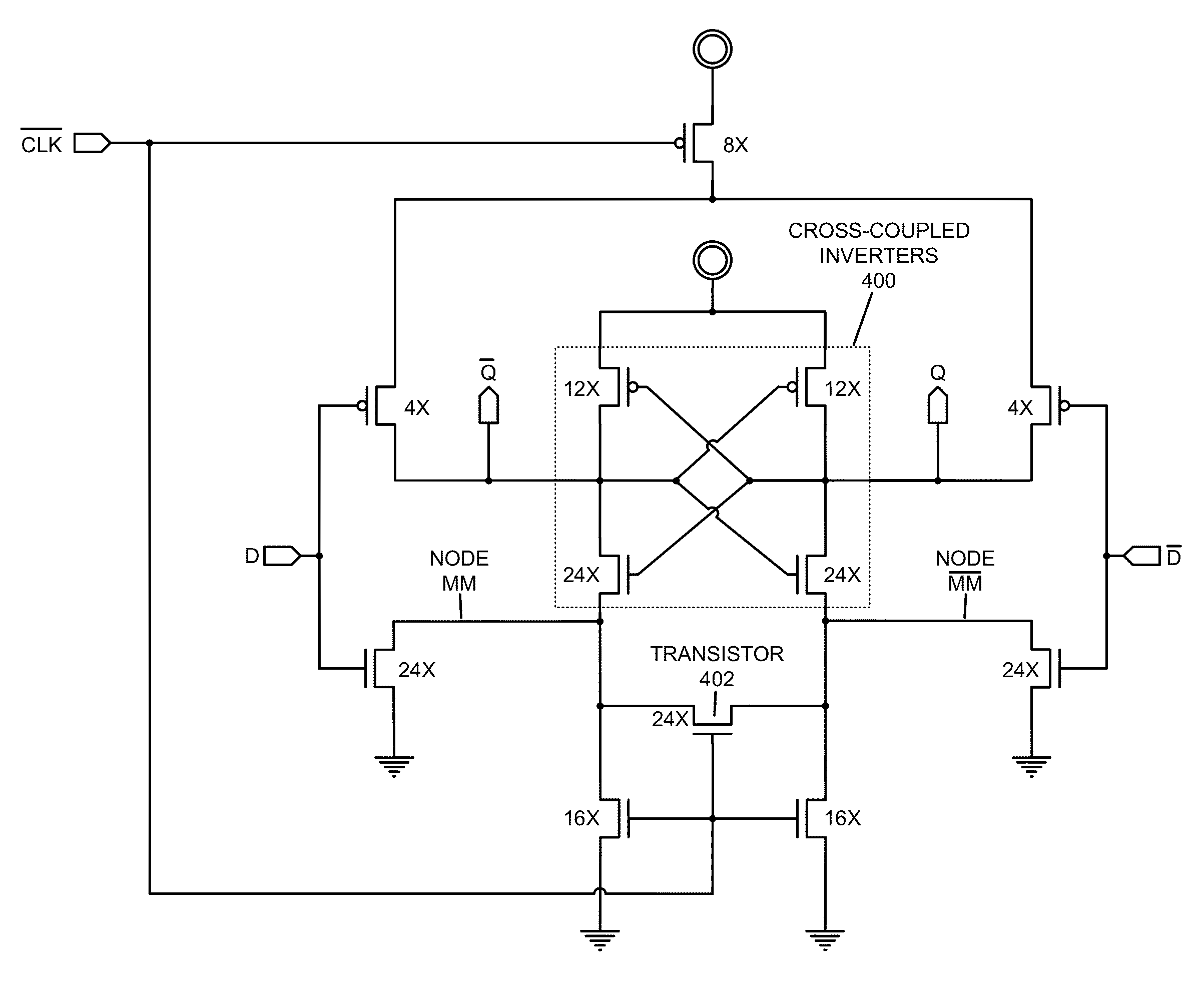
The disclosed embodiments provide a synchronizer latch circuit that facilitates resolving metastability issues. This synchronizer latch circuit includes a set of lightly loaded, cross-coupled transistors that form a metastable resolving and state-holding element that is coupled to two outputs. An incoming synchronization signal creates a voltage difference between the two outputs, but does not directly force a state change for the outputs. Instead, the data and clock inputs control transistors that allow neighboring power sources and / or ground network connections to weakly influence the outputs. The cross-coupled transistors then amplify the resulting voltage difference to generate valid output voltages, even when the data input and clock signal are received at roughly the same time. Thus, the synchronizer latch circuit facilitates rapidly resolving metastability and improving synchronizer performance.

Description

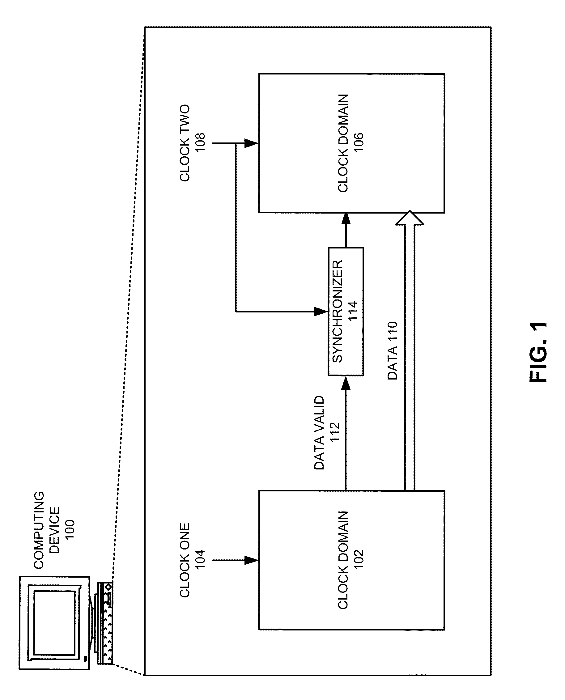
BACKGROUND[0001]1. Field of the Invention[0002]This disclosure generally relates to circuits and techniques for synchronizing signals from different clock domains. More specifically, this disclosure relates to circuits and techniques that resolve metastability issues while synchronizing signals.[0003]2. Related Art[0004]Clock signals are often distributed globally over an entire integrated circuit. However, as clock frequencies and the number of transistors on an integrated circuit continue to increase, implementing such global clock signals becomes increasingly difficult. Moreover, integrated circuits commonly contain different functional blocks that operate at different speeds. Consequently, many integrated circuits include multiple timing domains. In such integrated circuits, large numbers of synchronizing circuits (“synchronizers”) are often used to interface the different timing domains.[0005]Unfortunately, synchronizer performance does not scale at the same rate as logic-gate ...

Claims


Application Information

Patent Timeline
Patent Type & Authority Patents(United States)
IPC IPC(8): H03K3/356
CPCH03K3/356173H03K3/0375
Inventor JONES, IAN W.YANG, SUWENGREENSTREET, MARK R.GAYWALA, HETAL N.DROST, ROBERT J.
Owner ORACLE INT CORP
Learn More