Modular high density LED array light sources

a technology of led array light source and module, which is applied in the direction of printing, electrical equipment, lighting and heating apparatus, etc., can solve the problems of imposing constraints on system design, high amount of heat irradiated by gas discharge lamps, and often considered the most challenging combination of print quality and speed

Active Publication Date: 2013-11-12
EXCELITAS CANADA
View PDF1 Cites 18 Cited by
  • Summary
  • Abstract
  • Description
  • Claims
  • Application Information

AI Technical Summary

Benefits of technology

[0021]Preferably, the arrangement of LED die in each module provides for a substantially uniform irradiance from module to module where two modules abut.
[0023]In a preferred arrangement, each module comprises a central region the LED array arranged as a uniform periodic array of LED elements having a number n of die per unit length of the substrate, and an end region of the module near the edge of the array wherein die are arranged, so that, including the edge portion of the substrate extending beyond the LED array, there is an equal number n die per length of the substrate in end regions abutting other modules. Advantageously, the arrangement of LED die of the array in central and end regions of a module maximizes the packing density of individual die to provide a high intensity modular light source.
[0024]Thus, arrangements of LED die in each LED array provide for a substantially uniform irradiance where two modules abut, and reduce or overcome edge effects or wall effects, while preferably optimizing packing density for providing high optical power and irradiance in a single module.
[0026]Beneficially, the spacing of LED die in each middle cluster and end cluster, and the spacing between clusters is selected to provide high optical power and substantially uniform irradiance along the length of the array and across edge portions where two modules abut. For example, each middle cluster comprises at least one LED die and each end cluster comprises at least one additional LED die. Alternatively, each middle cluster comprises at least one pair of LED die, and each end cluster comprises at least one additional pair of die.
[0030]By appropriate selection of the number of die in each middle and end cluster, and spacing between clusters, a high optical power and a substantially uniform irradiance can be provided along the length of the array where two modules abut, to reduce or overcome edge effects or wall effects.

Problems solved by technology

Among these, the combination of print quality and speed is often considered most challenging.
However, the amount of heat irradiated from gas discharge lamps is usually very high, which places constraints on system design.
Overheating may cause operational and maintenance problems.
Excessive heat also limits the ability of inkjet printers to print on some heat sensitive substrates.
However, if the lamp power is lowered to avoid deleterious heating effects, there may be a trade off, e.g. in lower print quality and speed, or curing may not be achieved at all.
These arrangements may have difficulty in achieving a uniform beam profile and an intensity that is high enough for good print quality for some applications.
More densely packed LED chips may be provided to achieve high intensity, however water cooling may then be required which adds to the system complexity and cost.
An upper limit for irradiance of a densely packed LED array may also be limited by the packaging or mechanical housing of individual die that determines the minimum spacing between die.
With available LED arrays, for high speed printing applications using very short exposure times of the substrate to be cured, an array formed from individually packaged LED die, or a single row of LED die, may not provide sufficient intensity, and it is necessary to provide a higher density array to provide a line, a band, multiple lines, or multiple bands of illumination of higher intensity.
A problem encountered with available LED arrays, is that a linear array of a single row of individual LED die, for example, may be closely spaced along the row, but, because of the packaging and housing surrounding a linear array of individual die, when two arrays are abutted, the spacing between adjacent LED die, on different modules may be about 7 mm, for example, i.e. much larger than the spacing between dies on the same module (see FIG. 1B).
Thus, because of the thickness of the wall of the package or housing of available high density LED arrays and / or other design / assembly needs, there is a gap or spacing between LED die on neighbouring modules when they are abutted in a module assembly.
This means that there is uniform intensity along the length or width of the each module, but there is a dip in intensity / irradiance in the region where each module abuts, which tends to cause a banding effect in the substrate being cured.
However, neither of these applications addresses the problem of providing a more uniform irradiance profile where two modules abut.
However, because of the thickness of the substrate and packaging surrounding the array, this arrangement also does not overcome a discontinuity in irradiance around edges of the arrays, or where two arrays abut.
These photodetectors also take up space in the array, and add to expense.

Method used


Image

  • Modular high density LED array light sources
  • Modular high density LED array light sources
  • Modular high density LED array light sources

Examples


Embodiment Construction

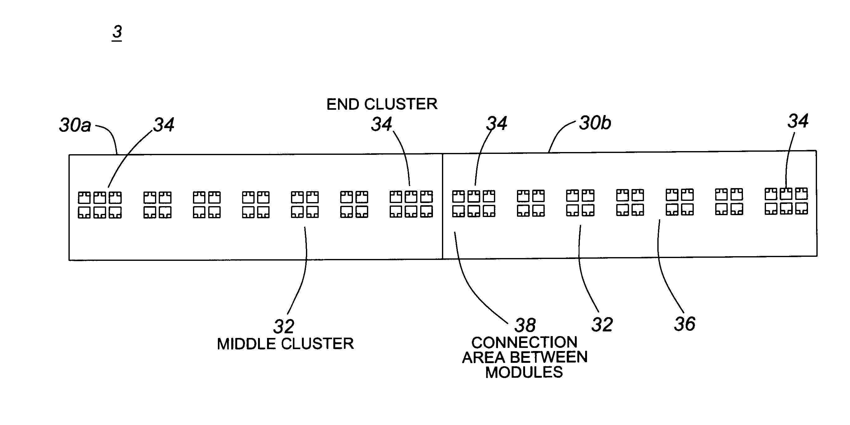
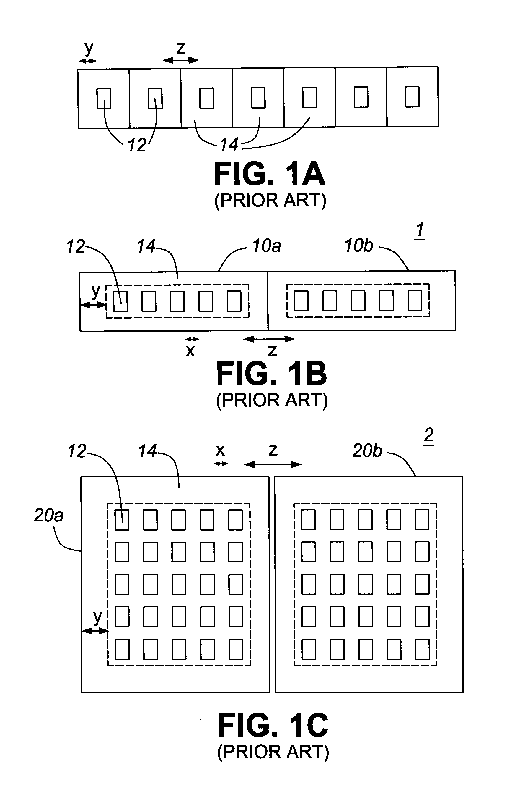
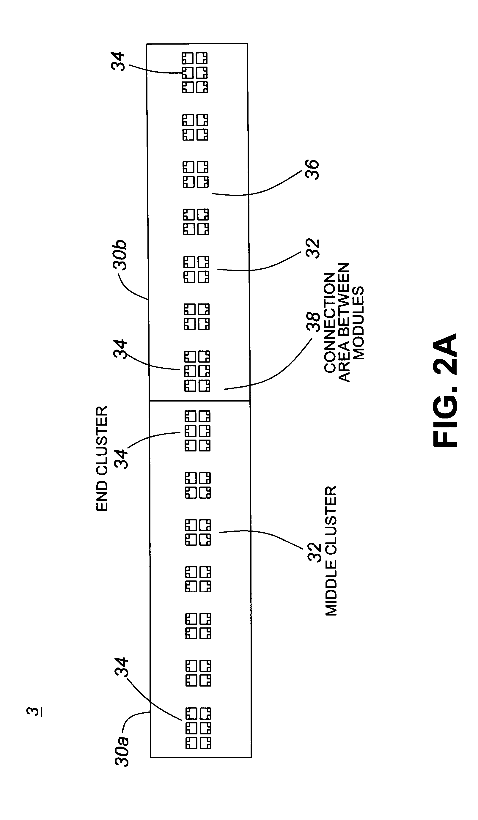
[0066]A conventional LED light source assembly comprising a plurality of off-the-shelf individually packaged LED elements or die 12, arranged uniformly in a linear array is shown schematically in FIG. 1A. For high intensity light source arrays, the die 12 are preferably closely spaced and packed as densely as possible, i.e. spaced by a distance z. However, the substrate 14 and individual packaging of each die 12 extends a distance y around each LED element, limiting the packing density of the die. To allow for a higher packing density, several die 12 may be mounted on a common substrate 14, to form an array module, e.g. module 10a, as shown in FIG. 1B. As shown schematically in FIG. 1B, a conventional modular LED die array light source 1 may comprise two or more LED modules 10a, 10b each comprising a plurality of LED die 12, in this case a 1×5 array, arranged uniformly in a linear array on a substrate 14. Correspondingly, a square or rectangular array 2 may be provided as shown sche...


PUM


Abstract

A modular LED array light source comprises an assembly of a plurality of solid-state LED array modules. Modules are abutted to provide a large area, high intensity and high-density array that provides substantially uniform irradiance. Preferably, in each module, a linear or rectangular array of groups of LED is provided in which the density of LED die in the array is higher at ends or edges of the modules abutting other modules, to provide improved uniformity of irradiance over the illuminated area between modules. Particular arrangements of clusters of LEDs are provided that reduce or overcome the discontinuity or dip in irradiance due to edge or wall effects caused by the spacing of LED die from edges of the substrate / packaging of each module. These arrangements are advantageous for hermetically sealed LED array modules, for example, which require a minimum wall thickness for an effective seal.

Description

CROSS-REFERENCE TO RELATED APPLICATIONS[0001]This application is related to U.S. patent application Ser. No. 61 / 139,203, entitled “System, method and adjustable lamp head assembly for Ultrafast UV curing” and U.S. patent application Ser. No. 61 / 161,281, entitled “Distributed Light Sources for Photo-reactive curing”, which are incorporated herein by reference.TECHNICAL FIELD[0002]This invention relates to array light sources, light source arrays comprising solid state light emitting devices (LEDs), and particularly to high density modular LED array light source for applications such as high speed printing and photocuring, and apparatus using LED array light sources.BACKGROUND[0003]Many inks, adhesives and other curable coatings comprise free radical based or cationic formulations which may be photo-cured by exposure to light, typically ultraviolet (UV) or short wavelength visible radiation. Applications include curing of large area coatings, adhesive curing, as well as the print proc...

Claims


Application Information

Patent Timeline
Patent Type & Authority Patents(United States)
IPC IPC(8): H01L33/00
CPCB41J2/45F21K9/00H01L25/0753H01L2924/0002H01L2924/00
Inventor KUK, SOLA ANNEWANG, YONGFARRELL, JAMES FRANCIS
Owner EXCELITAS CANADA
Why Eureka
Try Eureka