

Screening of polysilicon material and method of filling crucible
A polycrystalline silicon and crucible technology, applied in the growth field of single crystal silicon, can solve the problems of long exposure time of the furnace body, easy occurrence of gas, waste of crucible space, etc., so as to improve the efficiency of vibration screening, reduce the charging time, reduce the The effect of production costs
- Summary
- Abstract
- Description
- Claims
- Application Information
AI Technical Summary
Problems solved by technology
Method used
Image


Examples
Embodiment 1
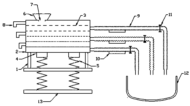
[0033] The unshaped polysilicon material obtained by the Siemens method is loaded into the hopper 6, and enters the screen 3 of the vibrating screen body 2 through the feed port 7, and the vibration motor 4 is started to automatically classify and screen the polysilicon material. Materials with a size below 55*55mm leak into the second layer of sieve through the holes of the first sieve for further screening, and materials with a size above 55*55mm that cannot pass through the sieve holes will remain on the sieve, and then pass through the left side The first outlet is used for collection; the aperture of the second layer of screen is 45*45mm, and the size smaller than 45*45mm leaks into the second layer of screen through the second layer of screen for further screening, and the size larger than 45*45mm The material will stay on the screen, and then enter the bellows from the right outlet for collection; with the above method, gradually pass through the third, fourth, and fifth...
PUM
| Property | Measurement | Unit |
|---|---|---|
| size | aaaaa | aaaaa |
Abstract
Description
Claims
Application Information