Solid-state image taking device and electronic apparatus

a technology of solid-state image and electronic equipment, which is applied in the direction of picture signal generators, television system scanning details, television systems, etc., can solve the problems of ktc noise and image quality degradation, and achieve the effect of eliminating noise components and eliminating noise components

Active Publication Date: 2014-01-07
SONY SEMICON SOLUTIONS CORP
View PDF12 Cites 1 Cited by
  • Summary
  • Abstract
  • Description
  • Claims
  • Application Information

AI Technical Summary

Benefits of technology

[0027]The kTC noise generated in the reset operation is a random noise caused by a switching operation carried out by the reset transistor 104 during the reset operation. Thus, if a level prior to the transfer of electric charge from the photodiode 101 to the floating diffusion capacitor FD is not used, the noise of the signal level cannot be eliminated with a high degree of accuracy. This is because the noise of the signal level is eliminated by carrying out the reset operation after the signal level has been read out as a level representing the amount of electric charge transferred from the photodiode 101 to the floating diffusion capacitor FD for all unit pixels at the same time. By getting rid of the noise in this way, a noise caused by an offset error or the like can be eliminated. However, the kTC noise cannot.
[0054]In accordance with the present invention, there is provided a solid-state image taking device capable of making noise components such as smear noise components, which have an effect on accumulated opto-electric charge, uniform throughout the layout surface of all unit pixels and also capable of sufficiently eliminating the noise components. In addition, also in accordance with the present invention, there are provided electronic apparatus each employing a solid-state image taking device capable of sufficiently eliminating noise components such as smear noise components.

Problems solved by technology

As a result, the quality of the image deteriorates.
However, the kTC noise cannot.

Method used


Image

  • Solid-state image taking device and electronic apparatus
  • Solid-state image taking device and electronic apparatus
  • Solid-state image taking device and electronic apparatus

Examples


second embodiment

2: Second Embodiment

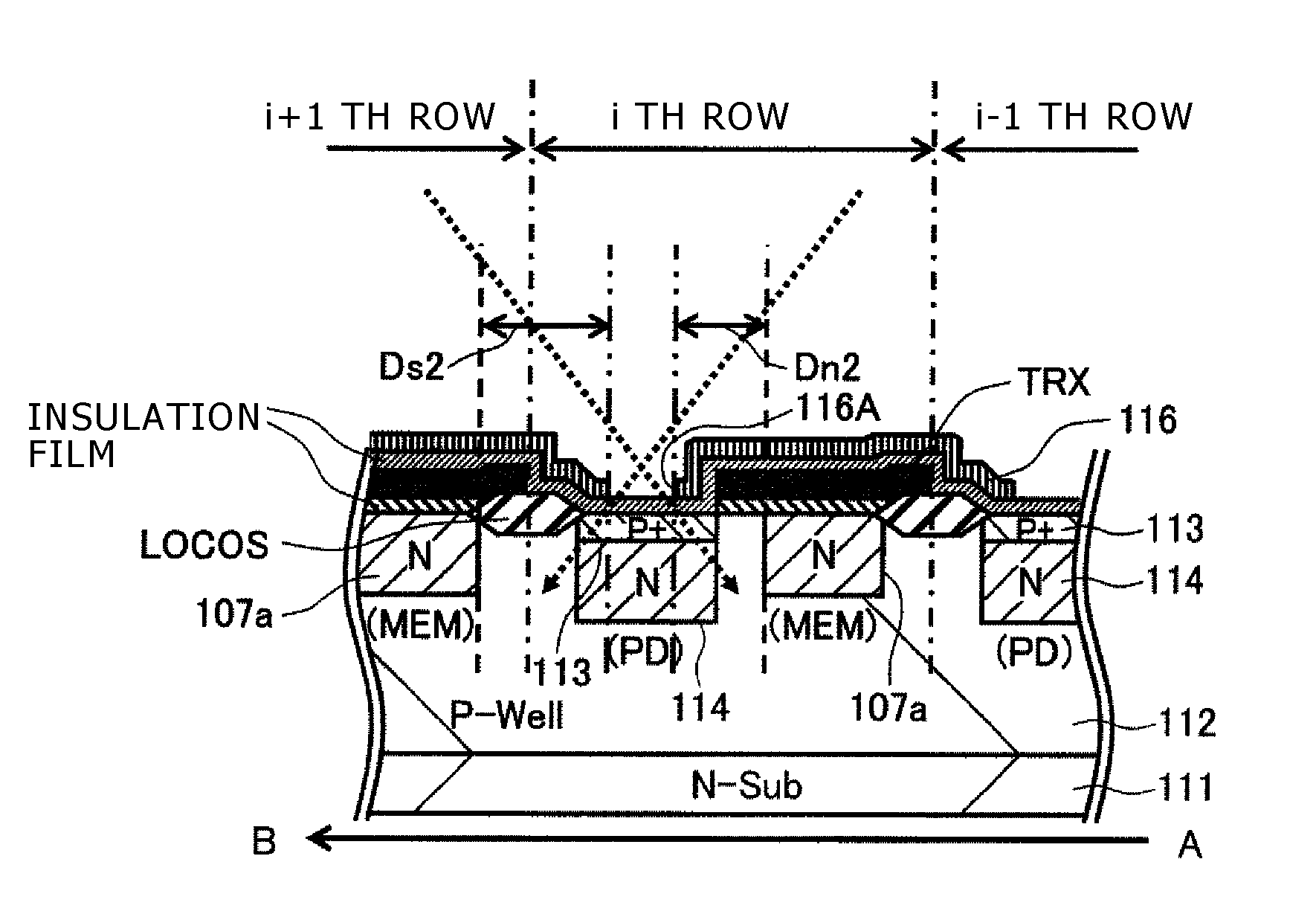
[0229]FIG. 20 is a pixel structure cross-sectional diagram referred to in the following description of a method for prescribing distances in accordance with the second embodiment. FIG. 20 is a diagram corresponding to FIG. 17 provided for the first embodiment. That is to say, FIG. 20 is a cross-sectional diagram showing a structure along a line A-B shown in FIG. 16. It is to be noted that FIGS. 10 to 16 provided for the first embodiment can also be applied to the second embodiment.

[0230]Much like FIG. 17, FIG. 20 shows a unit pixel on the ith pixel row at the center of the figure, a portion of a unit pixel on the (i−1)th pixel row on the right side of the figure and a portion of a unit pixel on the (i+1)th pixel row on the left side of the figure. The unit pixels are separated and insulated electrically from each other by an element separation layer prescribing an active layer mentioned before. In the structure shown in the figure, the element separation layer is...

third embodiment

3: Third Embodiment

[0234]FIG. 21 is a pixel structure cross-sectional diagram referred to in the following description of a method for prescribing distances in accordance with a third embodiment. FIG. 21 is a diagram corresponding to FIG. 17 provided for the first embodiment. That is to say, FIG. 21 is a cross-sectional diagram showing a structure along a line A-B shown in FIG. 16. It is to be noted that FIGS. 10 to 16 provided for the first embodiment can also be applied to the third embodiment.

[0235]Much like FIG. 17, FIG. 21 shows a unit pixel on the ith pixel row at the center of the figure, a portion of a unit pixel on the (i−1)th pixel row on the right side of the figure and a portion of a unit pixel on the (i+1)th pixel row on the left side of the figure. The unit pixels are separated and insulated electrically from each other by an element separation layer prescribing an active layer mentioned before. In the structure shown in the figure, the element separation layer is a LO...

fourth embodiment

4: Fourth Embodiment

[0242]Next, a fourth embodiment is explained by referring to FIGS. 22 to 26 as follows.

[0243]FIG. 22 is a top-view diagram showing the configuration of a unit pixel PIXB according to the fourth embodiment. FIG. 23 is a top-view diagram showing the basic configuration of a pixel array composed of unit pixels PIXB arranged to form a pixel matrix. The unit pixel PIXB has the pattern shown in FIG. 22. The basic configuration is a configuration for 6 unit pixels PIXB. The pixel array is the pixel array 11 employed in the CMOS image sensor 10 shown in FIG. 10. FIG. 24 is a top-view diagram showing a layout of light shielding films 116 for shielding the basic configuration of the pixel array shown in FIG. 23 against light and a layout of PD openings 116A each provided for one of the light shielding films 116. FIG. 25 is an explanatory top-view diagram showing the basic configuration of the pixel array for three scanned pixel rows each composed of unit pixels PIXB. FIG. ...


PUM


Abstract

Disclosed herein is a solid-state image taking device including a pixel section and a scan driving section wherein on each pixel column included in the pixel area determined in advance to serve as a pixel column having the unit pixels laid out in the scan direction, the opto-electric conversion section and the electric-charge holding section are laid out alternately and repeatedly, and on each of the pixel columns in the pixel area determined in advance, two the electric-charge holding sections of two adjacent ones of the unit pixels are laid out disproportionately toward one side of the scan direction with respect to the optical-path limiting section or the opto-electric conversion section.

Description

BACKGROUND OF THE INVENTION[0001]1. Field of the Invention[0002]The present invention relates to a solid-state image taking device adopting an all-pixel read method for reading out pieces of electric charge at the same time from opto-electrical conversion elements each employed in one of all unit pixels forming a pixel array and relates to an electronic apparatus in which the device is embedded.[0003]2. Description of the Related Art[0004]One of typical examples of the solid-state image taking device is a CMOS image sensor for reading out opto-electric charge, which has been accumulated in a PN junction capacitor of a photodiode serving as the opto-electric conversion element (also referred to hereafter as an opto-electric conversion section) of every unit pixel employed in the CMOS image sensor, through a MOS transistor of the pixel. The CMOS image sensor carries out an operation to read out pieces of opto-electric charge, which each have been accumulated in a photodiode, for every...

Claims


Application Information

Patent Timeline
Patent Type & Authority Patents(United States)
IPC IPC(8): H04N3/16H04N9/04
CPCH01L27/14603H01L27/14623H01L27/14612H01L27/1463H04N25/625H04N25/65H04N25/771H04N23/73H04N25/75H04N25/53H04N25/76
Inventor MACHIDA, TAKASHI
Owner SONY SEMICON SOLUTIONS CORP
Why Eureka
Try Eureka