Flash array built in self test engine with trace array and flash metric reporting

a self-testing and flash array technology, applied in the field of flash memory devices, can solve problems such as slow upda

Inactive Publication Date: 2014-01-07
GLOBALFOUNDRIES US INC
View PDF16 Cites 13 Cited by
  • Summary
  • Abstract
  • Description
  • Claims
  • Application Information

AI Technical Summary

Benefits of technology

[0009]According to an exemplary embodiment, a method for a flash array test engine circuit is provided. The method includes generating test workloads in a test mode for testing a flash device array, where each of the test workloads includes specific addresses, data, and command patterns to be sent to the flash device array. The method includes accelerating wear in the flash device array, via the test workloads, at an accelerated rate relative to general system workloads that are not part of the test mode. The method includes varying a range of conditions for the flash device array to determine whether each of the conditions passes or fails, and storing failure data and corresponding failure data address information for the flash device array.
[0010]According to an exemplary embodiment, a computer program product for a flash array test engine circuit is provided. The computer program product includes a computer readable storage medium having computer readable program code embodied therewith. The computer readable program code is configured for generating test workloads in a test mode for testing a flash device array, where each of the test workloads includes specific addresses, data, and command patterns to be sent to the flash device array. The computer readable program code is configured for accelerating wear in the flash device array, via the test workloads, at an accelerated rate relative to general system workloads that are not part of the test mode. The computer readable program code is configured for varying a range of conditions for the flash device array to determine whether each of the conditions passes or fails, and storing failure data and corresponding failure data address information for the flash device array.

Problems solved by technology

This makes it slow to update.

Method used


Image

  • Flash array built in self test engine with trace array and flash metric reporting
  • Flash array built in self test engine with trace array and flash metric reporting
  • Flash array built in self test engine with trace array and flash metric reporting

Examples


Embodiment Construction

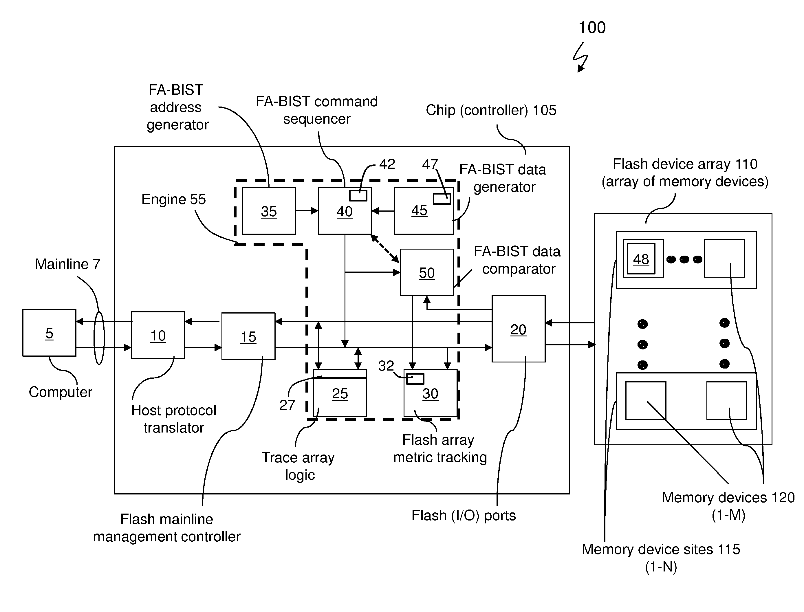
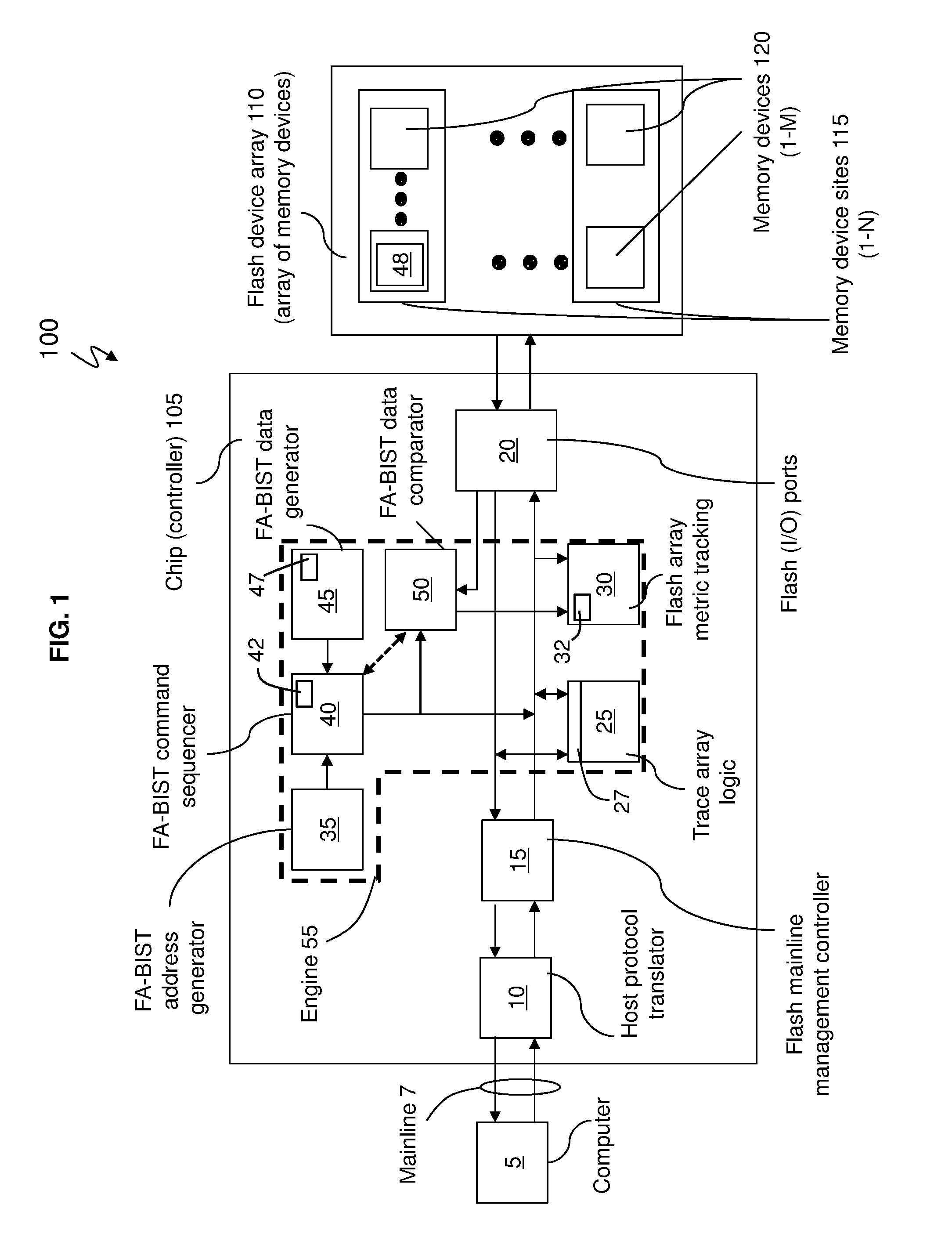
[0021]Exemplary embodiments are configured to provide a design that integrates into existing flash controller architectures and can be used during special test modes. Exemplary embodiments provide a controller chip (e.g., integrated circuit chip) with a flash array built in self test (FA-BIST) engine for testing an array of flash memory devices as shown in FIGS. 1 and 4. Typically, the flash array built in self test (FA-BIST) engine may be configured and invoked under debug conditions (e.g., during a test mode).

[0022]Integrating flash memory devices into a solid state drive (SSD) and / or into an existing flash (controller) design may have reliability and functional challenges. For example, in exemplary embodiments, the controller chip of the flash memory devices is configured to understand and account for the existing raw bit error rate in the flash memory devices on a per block basis, and understand / account for when the implemented error code correction (ECC) scheme (of the flash me...


PUM


Abstract

A mechanism is provided for a flash array test engine. The flash array test engine includes a circuit. The circuit is configured to generate test workloads in a test mode for testing a flash device array, where each of the test workloads includes specific addresses, data, and command patterns to be sent to the flash device array. The circuit is configured to accelerate wear in the flash device array, via the test workloads, at an accelerated rate relative to general system workloads that are not part of the test mode. The circuit is configured to vary a range of conditions for the flash device array to determine whether each of the conditions passes or fails and to store failure data and corresponding failure data address information for the flash device array.

Description

BACKGROUND[0001]Exemplary embodiments relate to flash memory devices, and more specifically, to performing built in self test of an array of flash memory cells.[0002]Flash memory is a nonvolatile computer storage chip that can be electrically erased and reprogrammed. It was developed from EEPROM (electrically erasable programmable read only memory) and must be erased in fairly large blocks before these can be rewritten with new data. The high density NAND (not and) type must also be programmed and read in (smaller) blocks, or pages, while the NOR (not or) type allows a single machine word (byte) to be written and / or read independently.[0003]The NAND type of flash memory is primarily used in memory cards, USB (universal serial bus) flash drives, solid state drives (SSD), and similar products, for general storage and transfer of data. The NOR type, which allows true random access and therefore direct code execution, is used as a replacement for the older EPROM and as an alternative to...

Claims


Application Information

Patent Timeline
Patent Type & Authority Patents(United States)
IPC IPC(8): G11C29/00
CPCG11C29/16G11C16/00G06F11/1068
Inventor CADIGAN, DAVID D.GRIFFIN, THOMAS J.SHETTY, ARCHANATRESSLER, GARY A.VANSTEE, DUSTIN J.
Owner GLOBALFOUNDRIES US INC
Why Eureka
Try Eureka