Thin film transistor array panel, liquid crystal display, and manufacturing method thereof

a technology of thin film transistor array panel and liquid crystal display, which is applied in the direction of instruments, semiconductor devices, optics, etc., can solve the problems of increasing the step between the data line and the pixel electrode, creating worsening errors during rubbing processes, so as to reduce incomplete rubbing or errors during rubbing, improve space uniformity, and reduce the effect of reducing the effective area ratio

Inactive Publication Date: 2014-03-04
SAMSUNG DISPLAY CO LTD
View PDF2 Cites 4 Cited by
  • Summary
  • Abstract
  • Description
  • Claims
  • Application Information

AI Technical Summary

Benefits of technology

[0012]Embodiments of the present invention provide a thin film transistor array panel, a liquid crystal display, and a manufacturing method therefor that allows for more complete rubbing, by eliminating or reducing a step difference in height between a pixel electrode and a data line, as well as the resulting light leakage.
[0013]Further, embodiments of the present invention provide a thin film transistor array panel, a liquid crystal display, and a manufacturing method therefor that can increase the effective area ratio of a spacer, i.e. the area of contact between a spacer and its opposing substrate.
[0014]In addition, embodiments of the present invention provide a thin film transistor array panel, a liquid crystal display, and a manufacturing method therefor that can prevent a short-circuit failure from occurring while a repair process is performed.
[0060]According to the exemplary embodiments of the present invention, a thin film transistor array panel, a liquid crystal display, and a manufacturing method therefor can prevent or reduce incomplete rubbing, or errors during rubbing, due to a step between a pixel electrode and a data line, and the resulting light leakage, by forming a step preventing member on the data line.
[0061]Further, it is possible to increase the effective area ratio, or the proportion of a spacer's area that contacts its opposing substrate, by forming the spacer on the thin film transistor array panel, thereby improving space uniformity between the two substrates of the liquid crystal display.
[0062]In addition, it is possible to prevent the thin film transistor array panel from being shorted-circuited via the common electrode during data line repair, as the spacers of the invention maintain more uniform spacing between the two substrates.

Problems solved by technology

This step can create errors during rubbing processes.
Furthermore, in structures in which a storage electrode is formed below the data line, the step between the data line and the pixel electrode grows even larger, worsening the errors during rubbing processes.
These errors can result in poor alignment of the liquid crystal, in turn resulting in light leakage between the data line and pixel electrode.

Method used


Image

  • Thin film transistor array panel, liquid crystal display, and manufacturing method thereof
  • Thin film transistor array panel, liquid crystal display, and manufacturing method thereof
  • Thin film transistor array panel, liquid crystal display, and manufacturing method thereof

Examples


Embodiment Construction

[0067]The present invention will be described more fully hereinafter with reference to the accompanying drawings, in which exemplary embodiments of the invention are shown. As those skilled in the art would realize, the described embodiments may be modified in various different ways, all without departing from the spirit or scope of the present invention.

[0068]In the drawings, the thickness of layers, films, panels, regions, etc., are exaggerated for clarity. Like reference numerals designate like elements throughout the specification. It will be understood that when an element such as a layer, film, region, or substrate is referred to as being “on” another element, it can be directly on the other element or intervening elements may also be present. In contrast, when an element is referred to as being “directly on” another element, there are no intervening elements present.

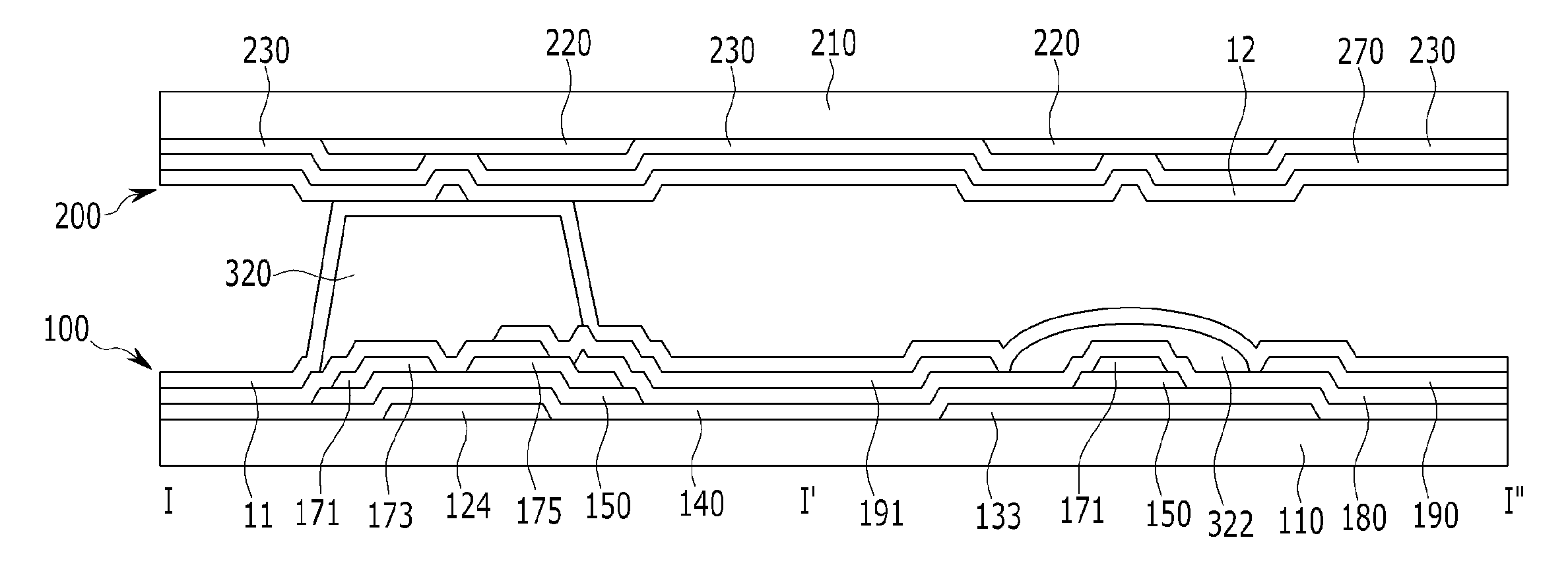
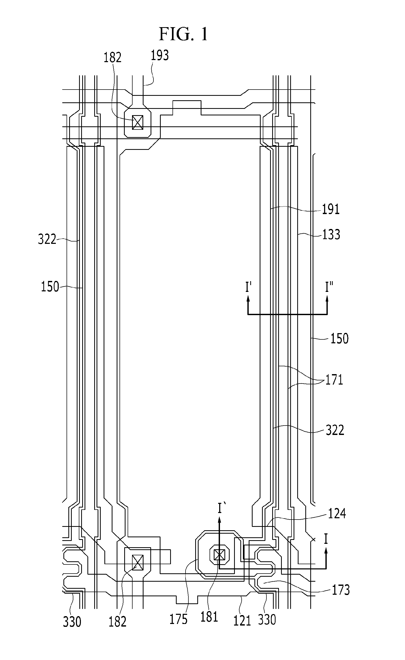
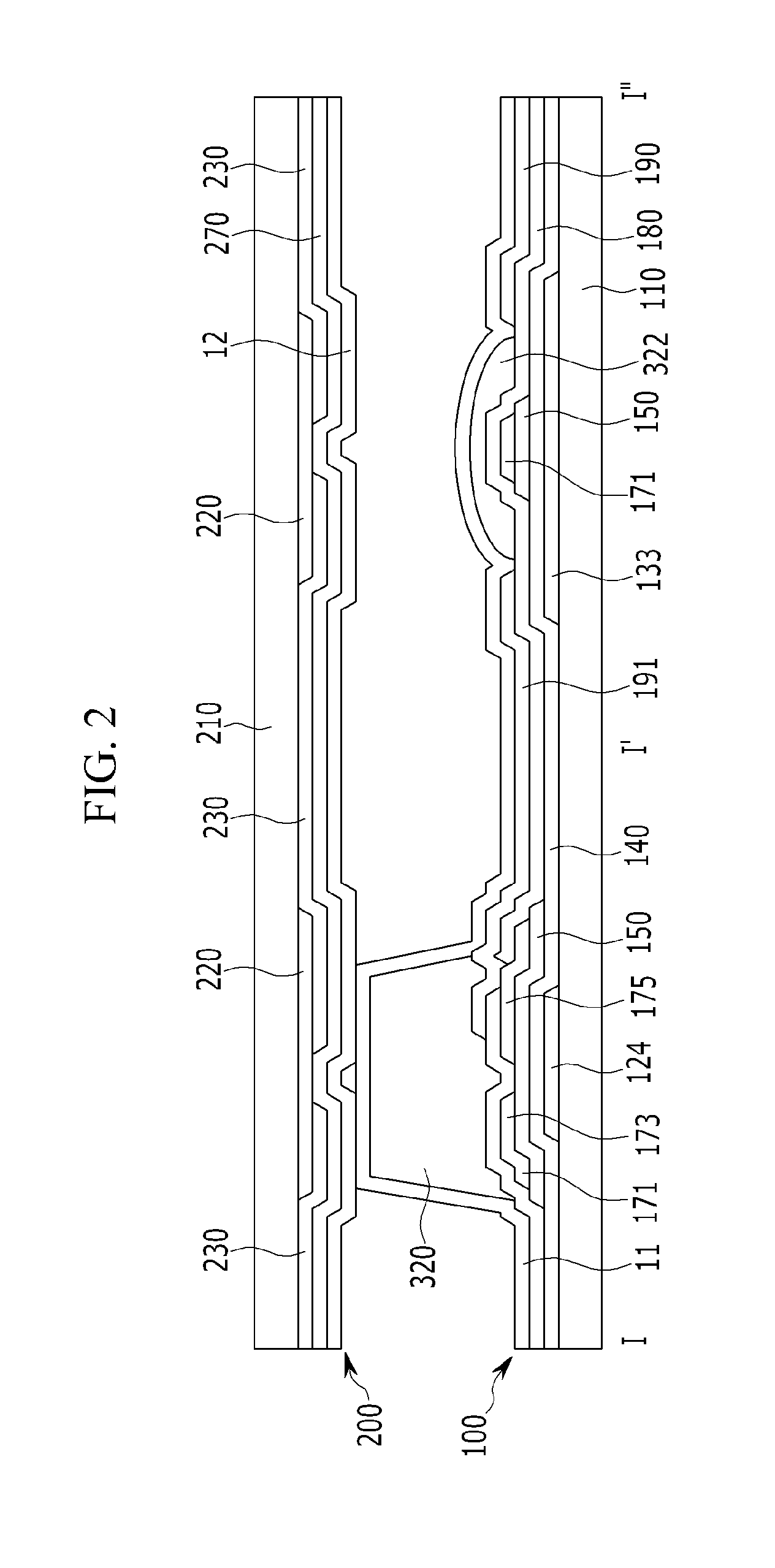
[0069]First, a liquid crystal display according to an exemplary embodiment of the present invention will be des...


PUM

PropertyMeasurementUnit
thicknessaaaaaaaaaa
widthaaaaaaaaaa
transparentaaaaaaaaaa

Abstract

Provided are a thin film transistor display panel, a liquid crystal display, and a manufacturing method therefor, that can prevent errors or omissions in rubbing due to a step between a pixel electrode and a data line, and the resulting light leakage, as well as increase the effective area ratio of a spacer and prevent shorts from occurring during at least some repair processes. The thin film transistor array panel includes: a first substrate; a gate line and a data line formed on the first substrate; a step preventing member formed on the data line to at least partially fill a volume positioned between the data line and a pixel electrode; and a spacer formed on the first substrate, wherein the spacer and the step preventing member comprise the same material.

Description

CROSS-REFERENCE TO RELATED APPLICATION[0001]This application claims priority to, and the benefit of, Korean Patent Application No. 10-2010-0103465 filed in the Korean Intellectual Property Office on Oct. 22, 2010, the entire contents of which are incorporated herein by reference.BACKGROUND OF THE INVENTION[0002](a) Field of the Invention[0003]Embodiments of the present invention relate generally to flat panel displays. More specifically, embodiments of the present invention relate to flat panel displays having improved rubbing and short circuit prevention characteristics.[0004](b) Description of the Related Art[0005]A liquid crystal display, as one type of flat panel display that is finding wide acceptance at present, typically includes two display panels on which electric field generating electrodes (such as a pixel electrode) and a common electrode are formed, with a liquid crystal layer interposed therebetween. The display crystal display generates an electric field in the liquid...

Claims


Application Information

Patent Timeline
Patent Type & Authority Patents(United States)
IPC IPC(8): G02F1/1339
CPCG02F1/13392H01L27/124G02F1/13394G02F1/136286G02F2201/48G02F1/133784G02F1/134336G02F1/136277G02F1/133519G02F1/13625
Inventor LEE, MYUNG SUBJEONG, JI YOUNGJOO, SUN-KYULEE, MYUNG JIN
Owner SAMSUNG DISPLAY CO LTD
Why Eureka
Try Eureka