Progressive trimming method

a cutting method and progress technology, applied in the direction of grinding machines, grinding/polishing apparatus, manufacturing tools, etc., can solve the problems of limited heat and/or stress during the second trimming step, and achieve the effect of minimizing the risk of delamination

Active Publication Date: 2014-03-25
SOITEC SA
View PDF77 Cites 15 Cited by
  • Summary
  • Abstract
  • Description
  • Claims
  • Application Information

AI Technical Summary

Benefits of technology

[0012]Thus, by carrying out a first trimming step as close as possible to the edge of the first wafer and over a predetermined width, the first wafer is attacked while remaining relatively far away from the components thereof. This limits heating and / or stresses in the structure even when trimming is intense, i.e. penetrating significantly into the second wafer.
[0014]As a result, the two trimming steps of the method of the invention mean that complete trimming of at least the first wafer can be carried out while substantially reducing the phenomena of macro and micro peel-off that normally appear during single-step trimming.
[0020]The use of the trimming method of the invention means that three-dimensional structures can be produced by stacking two or more wafers, minimizing the risks of delamination both at the bonding interfaces between the wafers and at the component layers. One of the component layers may include image sensors.

Problems solved by technology

Further, the heating and / or stresses are also limited during the second trimming step, even though said second trimming step is carried out at a distance that is further from the edge of the first wafer, i.e. close to the components.

Method used


Image

  • Progressive trimming method
  • Progressive trimming method
  • Progressive trimming method

Examples


Embodiment Construction

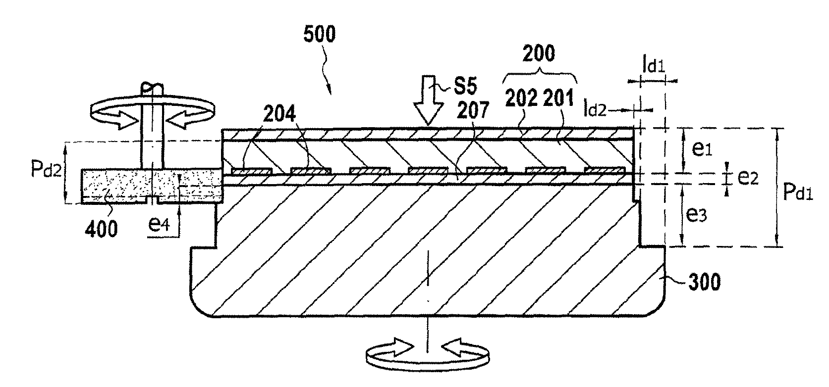
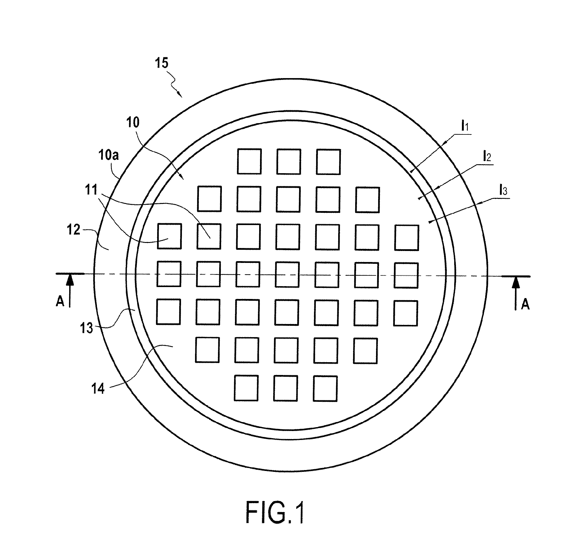
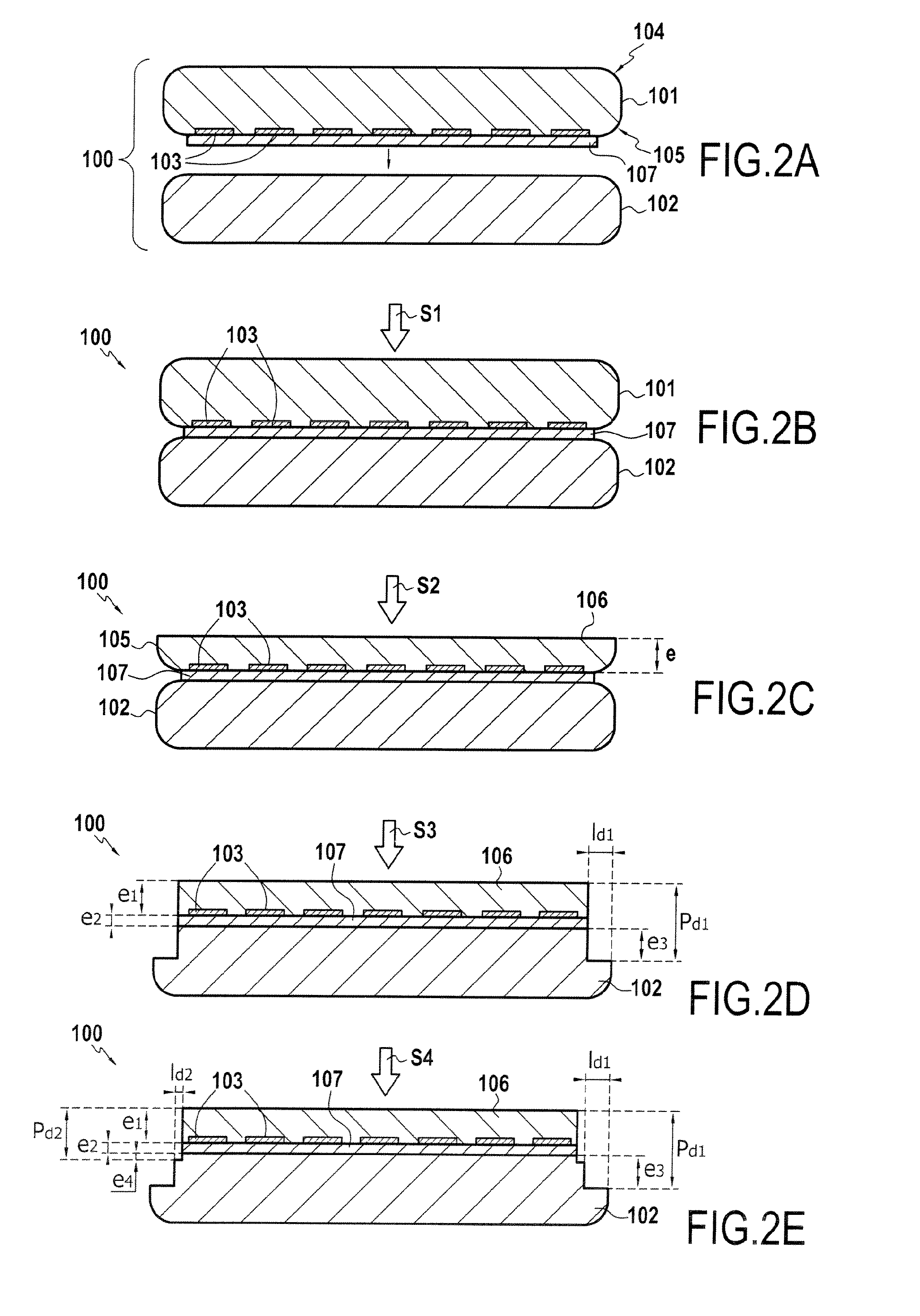
[0027]The present invention is of general application to trimming a structure comprising at least two wafers assembled together by molecular bonding or any other type of bonding such as anodic bonding, metallic bonding, or bonding with adhesive, it being possible for components to be formed beforehand in the first wafer that is then bonded to the second wafer that constitutes a support. The wafers are generally of circular outline, possibly with different diameters, in particular diameters of 100 millimeters (mm), 200 mm, or 300 mm. The term “components” as used here means any type of element produced with materials that differ from the material of the wafer and that are sensitive to the high temperatures normally used to reinforce the bonding interface. These components correspond in particular to elements forming all or a portion of an electronic component or a plurality of electronic microcomponents, such as circuits or contacts or active layers that may be damaged or even destro...


PUM

PropertyMeasurementUnit
thicknessaaaaaaaaaa
thicknessaaaaaaaaaa
diameteraaaaaaaaaa

Abstract

The invention provides a method of trimming a structure that includes a first wafer bonded to a second wafer, with the first wafer having a chamfered edge. The method includes a first trimming step carried out over a first depth that includes at least the thickness of the first wafer and over a first width determined from the edge of the first wafer. A second trimming step is then carried out over a second depth that includes at least the thickness of the first wafer and over a second width that is less than the first width.

Description

[0001]This application is a 371 filing of International Patent Application PCT / EP2009 / 059961 filed Jul. 31, 2009.FIELD OF THE INVENTION AND PRIOR ART[0002]The present invention relates to the field of producing multilayer semiconductor structures or substrates (also termed multilayer semiconductor wafers) produced by transfer of at least one layer onto a support. The transferred layer is formed by molecular bonding of a first wafer onto a second wafer or support, the first wafer generally being thinned following bonding. The first wafer may also include all or part of a component or a plurality of microcomponents, as happens with three-dimensional (3D) integration of components, which requires transfer of one or more layers of microcomponents onto a final support, and also as happens with circuit transfer as, for example, in the fabrication of back lit imaging devices.[0003]The edges of the wafers used to form the transferred layers and the supports generally have chamfers or edge r...

Claims


Application Information

Patent Timeline
Patent Type & Authority Patents(United States)
IPC IPC(8): H01L21/46H01L21/30
CPCH01L21/304H01L2225/06513H01L2924/0002H01L25/50H01L21/76256H01L2924/00
Inventor BROEKAART, MARCELMIGETTE, MARIONMOLINARI, SEBASTIENNEYRET, ERIC
Owner SOITEC SA
Why Eureka
Try Eureka