
Synchronized and shortened master-slave RF pulsing in a plasma processing chamber

a plasma processing chamber and master-slave technology, applied in process and machine control, electric variable regulation, instruments, etc., can solve problems such as electrical stress between features and layers of wafers, device damage, and undercutting features after etching

Active Publication Date: 2014-04-08
LAM RES CORP
View PDF31 Cites 16 Cited by
  • Summary
  • Abstract
  • Description
  • Claims
  • Application Information

AI Technical Summary

Benefits of technology

The patent text discusses the use of plasma processing in the production of electronic products. However, the charged species in the plasma can cause damage to the substrate and create electrical stress on the features formed on the substrate surface. The technical effect of the patent is to provide a method for processing substrates using plasma without causing damage or electrical stress. This is achieved by pulsating the RF energy source or both the source and the bias RF power supply, which can create an afterglow period during which the charged species have a reduced effect on the substrate. The method can also involve using multiple RF frequencies and synchronizing or asynchronizing the pulses of the RF power supplies.

Problems solved by technology

This electrical charge on the wafer may, in some cases, undesirably result in the alteration of the desired topography of the features and may even lead to device damage.
For example, charged species may be attracted to or repelled from the charged sidewalls of features on the wafer surface, resulting in undercut features after the etch is completed.
The electrical charge on the wafer may also cause electrical stress among features and layers of the wafer.
Furthermore, energetic charged and neutral species striking the charged wafer may cause structural damage (such as voids or dislocations) to features formed in the upper layer of the wafer.
Accordingly, useful processing in the afterglow state tends to be limited in duration.
The high bias condition, which is characterized by a high bias voltage existing on the chuck in the absence of a high density plasma in the chamber, may cause particles and / or species to impact the chuck and / or the wafer at high velocity, leading to bombardment damage.
This high bias condition, as mentioned, may potentially damage the wafer and / or the chuck due to excessive bombardment.

Method used


Image

  • Synchronized and shortened master-slave RF pulsing in a plasma processing chamber
  • Synchronized and shortened master-slave RF pulsing in a plasma processing chamber
  • Synchronized and shortened master-slave RF pulsing in a plasma processing chamber

Examples


Embodiment Construction

[0019]The present invention will now be described in detail with reference to a few embodiments thereof as illustrated in the accompanying drawings. In the following description, numerous specific details are set forth in order to provide a thorough understanding of the present invention. It will be apparent, however, to one skilled in the art, that the present invention may be practiced without some or all of these specific details. In other instances, well known process steps and / or structures have not been described in detail in order to not unnecessarily obscure the present invention.

[0020]Various embodiments are described hereinbelow, including methods and techniques. It should be kept in mind that the invention might also cover articles of manufacture that includes a computer readable medium on which computer-readable instructions for carrying out embodiments of the inventive technique are stored. The computer readable medium may include, for example, semiconductor, magnetic, ...


PUM


Abstract

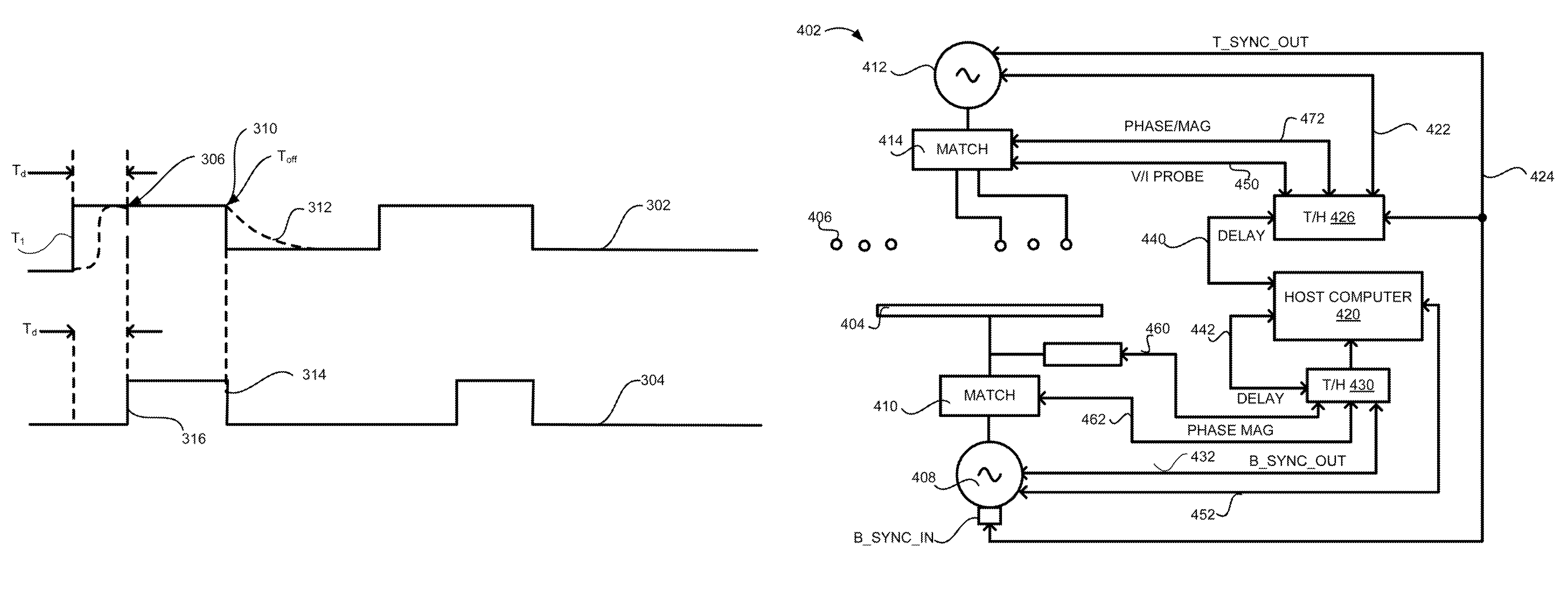
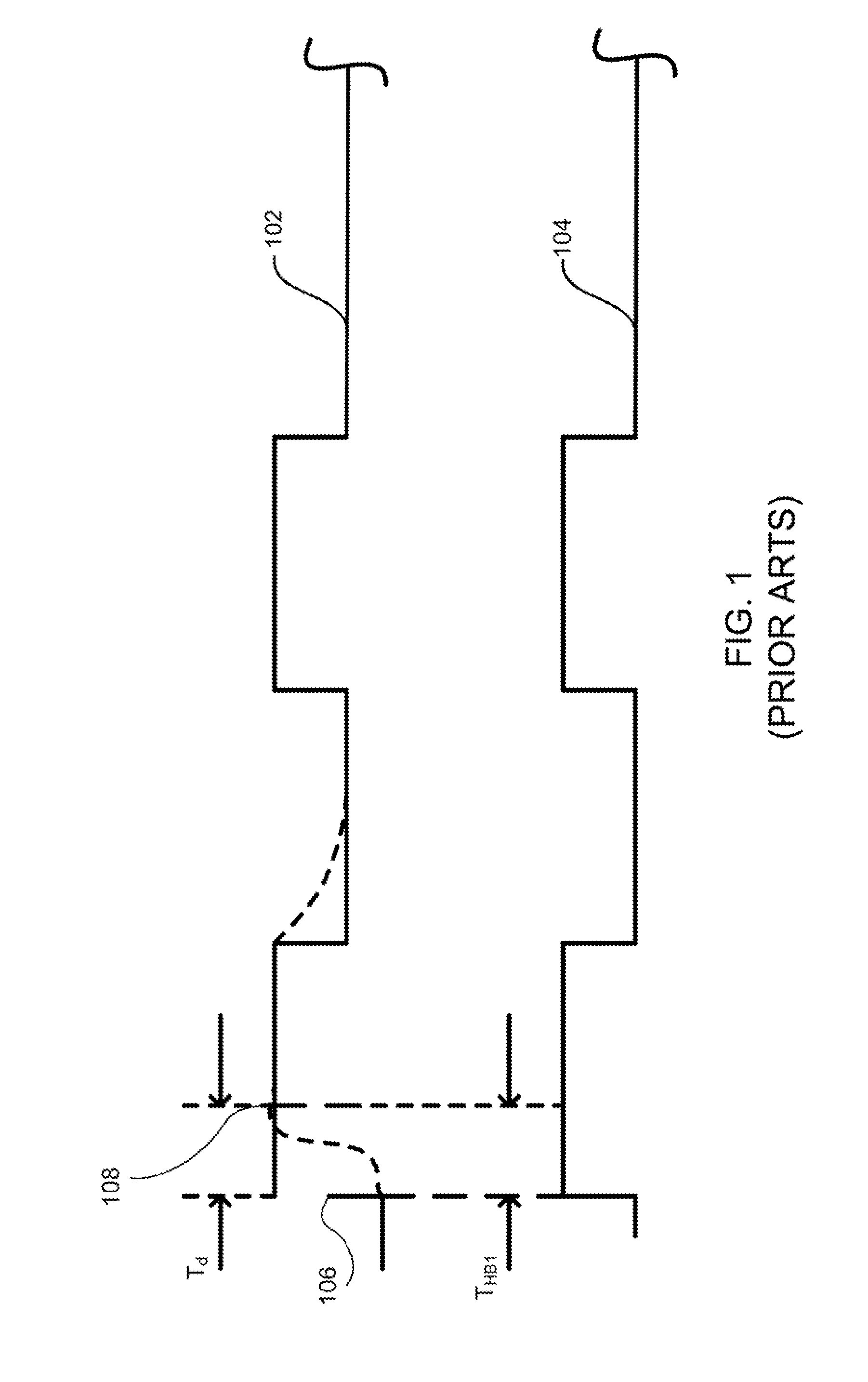
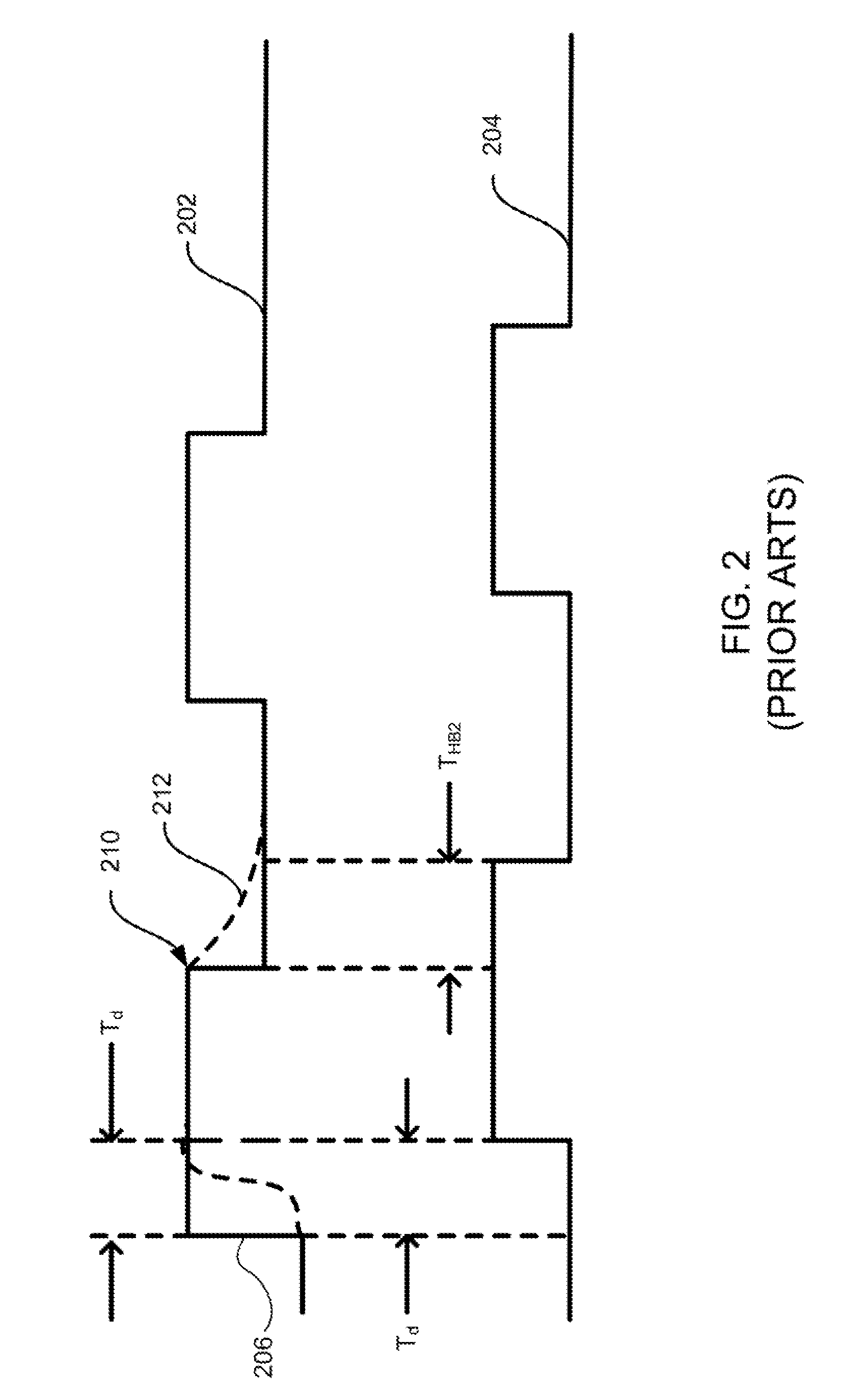
Plasma processing apparatuses and techniques for processing substrates, which include the use of synchronized RF pulsing of a first RF signal and a delayed-and-shortened second RF signal. The first RF signal may be the primary plasma-generating RF signal and the second RF signal may be the RF bias signal or vice versa. Alternatively or additionally, the first RF signal may be the high frequency RF signal and the second RF signal may be the lower frequency RF signal. Either the first RF signal or the second RF signal may act as the master, with the other acting as the slave signal. Alternatively, an external circuit may be employed as a master to control both the first RF signal and the second RF signal as slave signals. Track-and-hold techniques and circuits are provided to ensure accurate measurement for process control and other purposes.

Description

BACKGROUND OF THE INVENTION[0001]Plasma has long been employed to process substrates (e.g., wafers or glass panels) to produce electronic products (e.g., integrated circuits or flat panel displays). In the processing of a substrate, plasma may be employed to etch or deposit material. Generally speaking, plasma processing involves disposing a substrate on a suitable work piece holder, such as a chuck. An RF (radio frequency) energy source may be employed to ignite a process source gas inside a plasma processing chamber, forming a plasma for processing the substrate. In the case of an inductively coupled plasma processing chamber, this RF plasma-generation energy source is typically implemented by an RF power supply supplying RF energy to an inductive coil. In the following discussion, wafers and inductively coupled plasma processing chambers are employed as examples. It should be understood, however, that the invention is not limited to these particular examples.[0002]When the RF ene...

Claims


Application Information

Patent Timeline
Patent Type & Authority Patents(United States)
IPC IPC(8): H01J7/24
CPCH01J37/32082H01J37/32137H01J37/32146H01J37/32935
Inventor BENJAMIN, NEIL MARTIN PAULSATO, ARTHUR H.
Owner LAM RES CORP
Learn More