

Photo-coupler device
a photo-coupler and photo-coupler technology, applied in the field of photo-coupler devices, can solve the problems of poor voltage conversion efficiency and common-mode transient resistance, inaccurate reception signals, and easy reduction of electrical conductivity of the photo-coupler structure, and achieve low resistance values, good transmittance, and good voltage conversion efficiency
- Summary
- Abstract
- Description
- Claims
- Application Information
AI Technical Summary
Benefits of technology
Problems solved by technology
Method used
Image

Examples
first embodiment
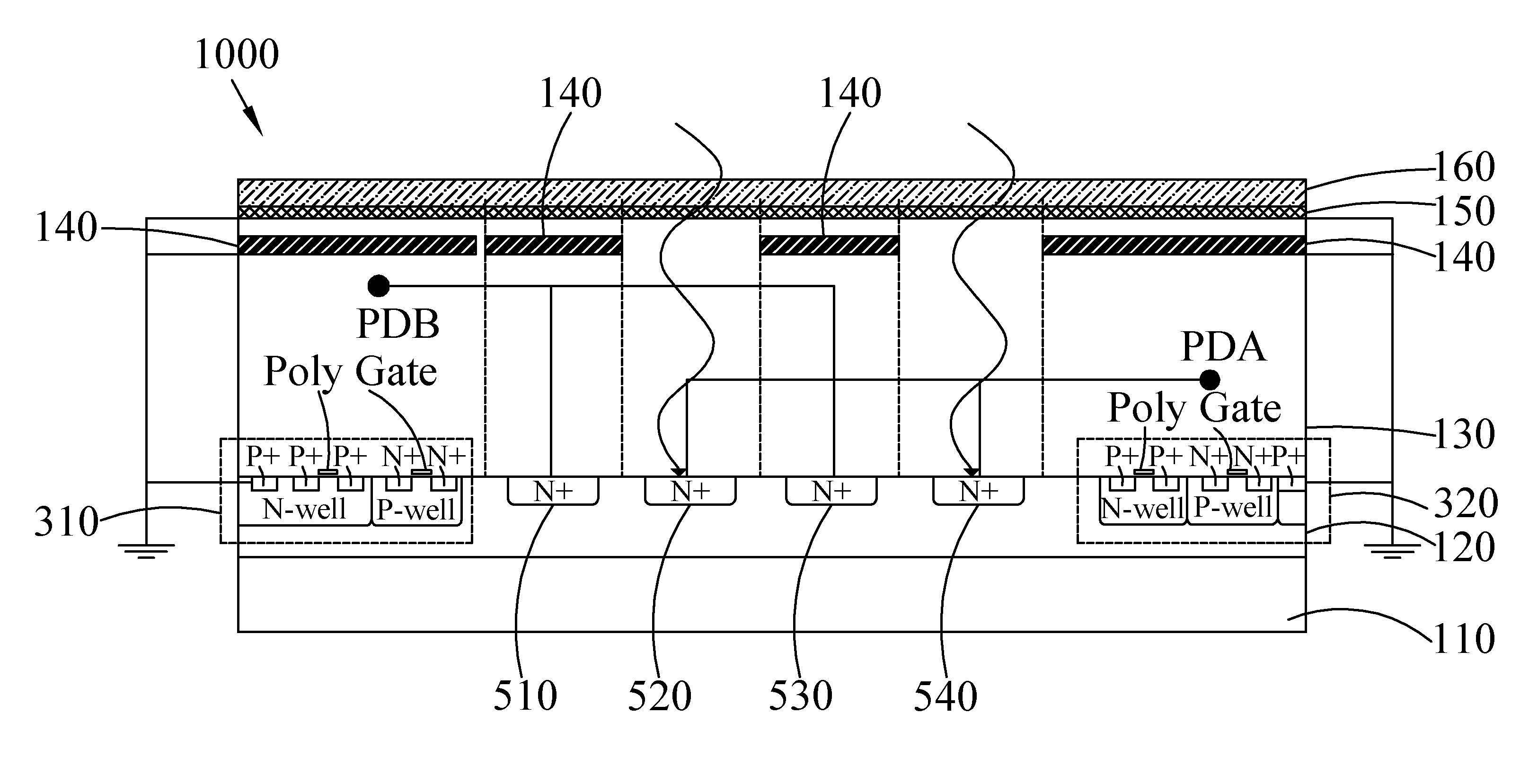
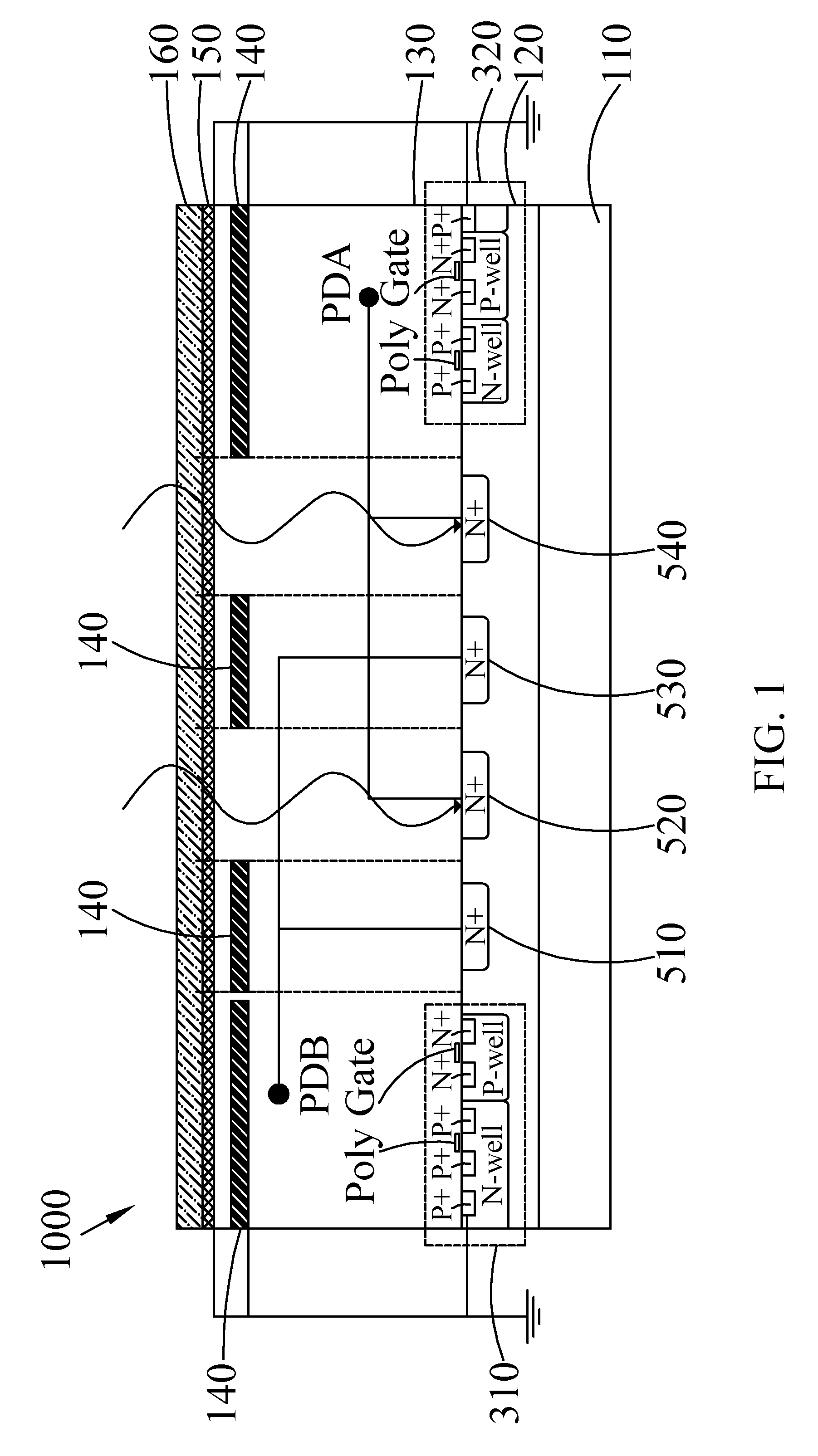
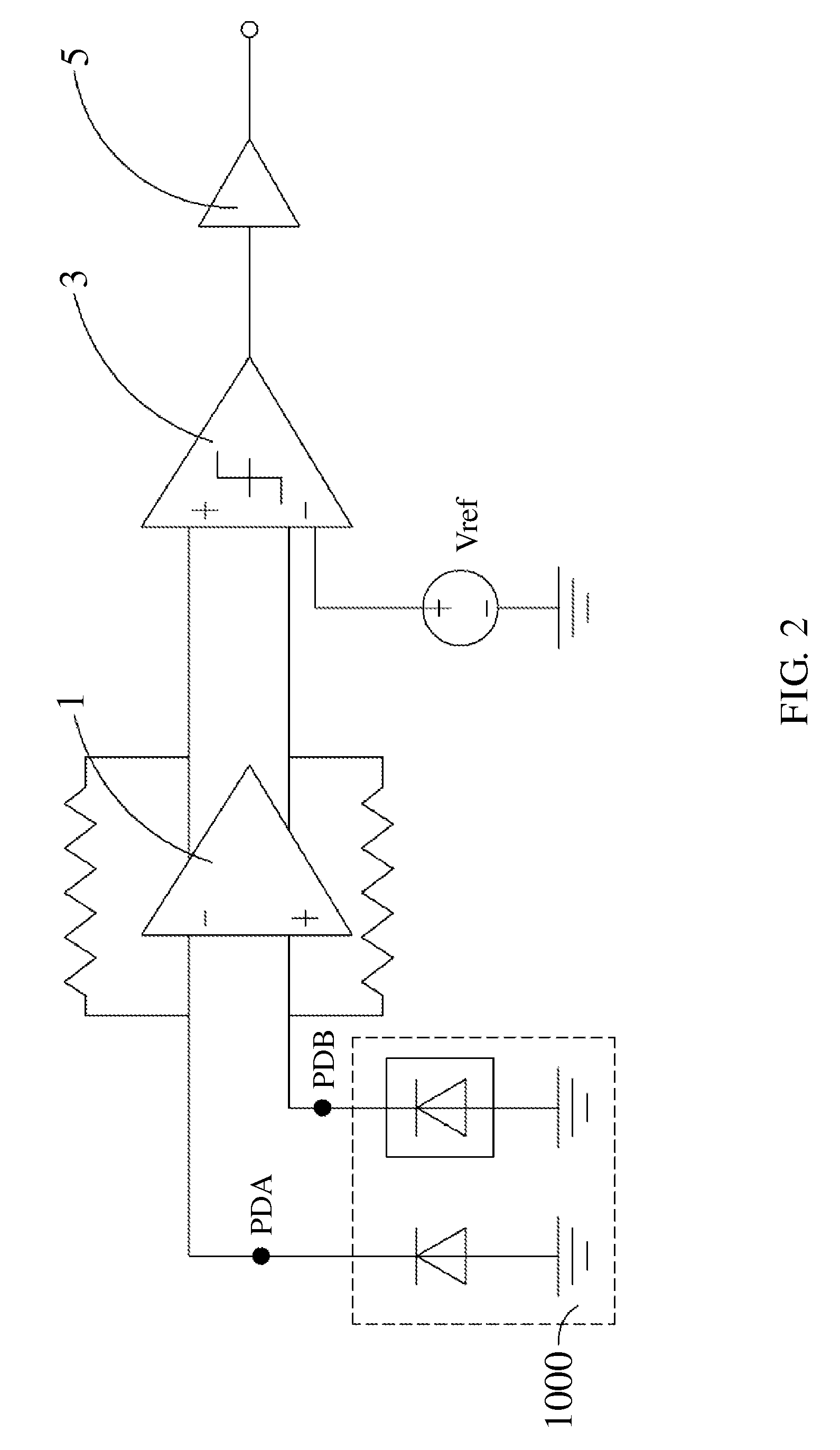
[0036]With reference to FIG. 1, in which a schematic diagram of the photo-coupler device according to the present invention is depicted. In FIG. 1, the photo-coupler device 1000 comprises a P-type substrate 110, a P-type epitaxial layer 120, an insulating layer 130, a plurality of shielding layers 140, a metal layer 150 and a passivation layer 160. The P-type epitaxial layer 120 is deposited on the P-type substrate 110. The insulating layer 130 is deposited on the P-type epitaxial layer 120. The shielding layers 140 are deposited in the insulation layer 130 in parallel in a horizontal direction. The metal layer 150 is deposited on the insulation layers 130. The passivation layer 160 is deposited on the metal layer 150.
[0037]The P-type epitaxial layer 120 further comprises two conducting regions 310, 320 and a plurality of N+ electrode regions between the two conducting regions 310, 320, and in which two of the shielding layers 140 are correspondingly arranged for covering the two co...
second embodiment
[0045]With reference to FIG. 3, in which a schematic diagram of the photo-coupler device according to the present invention is depicted. In the embodiment, the photo-coupler device 2000 comprises a P-type substrate 210, a P-type epitaxial layer 220, an insulating layer 230, a plurality of shielding layers 240, a metal layer 250 and a passivation layer 260. The P-type epitaxial layer 220 is deposited on the P-type substrate 210. The insulating layer 230 is deposited on the P-type epitaxial layer 220. The shielding layers 240 are deposited in the insulation layer 230 in parallel in a horizontal direction. The metal layer 250 is deposited on the insulation layers 230. The passivation layer 260 is deposited on the metal layer 250.
[0046]According to the above, the P-type epitaxial layer 220 further comprises two conducting regions 410, 420 and a plurality of N+ electrode regions between the two conducting regions 410, 420. Wherein, the plurality of shielding layers 240 correspondingly co...
PUM
 Abstract
Description
Claims
Application Information