Semiconductor device
A semiconductor and device technology, applied in the field of semiconductor devices with power circuits, to achieve the effect of improving voltage conversion efficiency and reducing parasitic wiring inductance
- Summary
- Abstract
- Description
- Claims
- Application Information
AI Technical Summary
Problems solved by technology
Method used
Image
Examples
no. 1 example
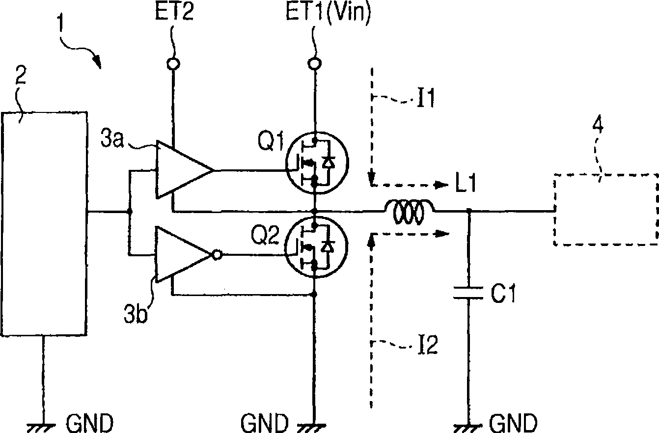
[0050] The semiconductor device according to the first embodiment of the present invention is a non-isolated DC-DC converter for a power supply circuit used in, for example, a desktop personal computer, a notebook personal computer, a server, or a game machine. figure 1 It is a circuit diagram showing an example of the non-isolated DC-DC converter 1. The non-isolated DC-DC converter 1 includes: a control circuit 2, driver circuits 3a, 3b, a power MOSFET Q1 (first field effect transistor), a power MOSFET Q2 (second field effect transistor), a coil L1 and a capacitor C1. These elements are mounted on a wiring substrate and electrically interconnected by wiring on the wiring substrate. figure 1 Reference numeral 4 in indicates a CPU (Central Processing Unit), DSP (Digital Signal Processor) or other load circuit used in the above-mentioned desktop personal computer, notebook personal computer, server, game machine, etc. Reference marks ET1 and ET2 indicate terminals.
[0051] The con...
no. 2 example
[0086] Now, a second embodiment of the non-isolated DC-DC converter 1 according to the present invention will be described. Figure 20 It is a plan view illustrating a typical structure of the package 6a, which includes a part of the circuit for the non-isolated DC-DC converter 1. Figure 21 show Figure 20 The Y1-Y1 section. In order to improve the visibility of the drawings, Figure 20 Part of the shell 8 is excluded. In addition, the die pads 7a1 and 7a2 and the lead 7b are shaded.
[0087] In the second embodiment, the wiring for connecting the pad BP and each part is partially changed from the wire WR to the metal plate wire 30. More specifically, the pad BP1 for the drain of the power MOSFET Q1 in the semiconductor chip 5a is electrically connected to the lead 7b1 via a metal plate wire 30. The pad BP2 used for the source of the power MOSFET Q1 in the semiconductor chip 5a is electrically connected to the die pad 7a2 via the metal plate wire 30. The pad BP6 for the source of...
no. 3 example
[0090] Now, a third embodiment of the non-isolated DC-DC converter 1 according to the present invention will be described. Figure 22 It is a plan view illustrating a typical structure of the package 6a, which includes a part of the circuit for the non-isolated DC-DC converter 1. Figure 23 show Figure 22 The Y1-Y1 section. In order to improve the visibility of the drawings, Figure 22 Part of the shell 8 is excluded. In addition, the die pads 7a1 and 7a2 and the lead 7b are shaded.
[0091] In the third embodiment, the wiring for connecting the pad BP and each part is partially changed from the above-mentioned wire WR to the ribbon wire 33. The connection of the ribbon wire 33 is not described here because they are the same as the connection of the metal plate wire 30 used in the second embodiment. For example, the ribbon wire 33 is formed of copper (Cu), aluminum (Al), or other similar metals that are the same as in the case of the metal plate wire 30 described above. However, ...
PUM
 Abstract
Description
Claims
Application Information


