Electro-optic device

a technology of optical devices and optical polarization, applied in the field of optical polarization devices, can solve the problems of reducing the efficiency of optical polarization, and reducing the loss of so as to improve humidity resistance and reduce optical polarization and rf wave propagation. the effect of loss reduction

Active Publication Date: 2014-07-08
LUMENTUM OPERATIONS LLC
View PDF12 Cites 5 Cited by
  • Summary
  • Abstract
  • Description
  • Claims
  • Application Information

AI Technical Summary

Benefits of technology

[0026]In one embodiment of the invention, the RF signal electrode is used as a bias ground electrode. Thus, for Z-cut electro-optic crystals, there is no need to place a buried bias electrode under the RF signal electrode and over the optical waveguide. As a result, both optical and the RF wave propagation losses are reduced. Since the RF signal electrode is used as a bias ground electrode, its potential is zero, which improves humidity resistance as well. In another embodiment, a buried bias electrode is placed over the optical waveguide between two buffer layers having different electrical conductivity. The buffer layer on top of the buried bias electrode has a smaller electrical conductivity than the buffer layer below the buried bias electrode. This reduces voltage drops due to leakage currents.
[0031]In one embodiment, the bias electrode is disposed not under but over the buffer layer, to reduce leakage currents.

Problems solved by technology

Unfortunately, Z-cut LiNbO3 modulators are also known to suffer more from charge build up problems, which may lead to temperature-induced bias drift and / or a DC-induced bias drift.
Unfortunately, to accommodate both electrode structures, the length of the modulator has to be significantly increased.
In addition, it is not ideal to locate the waveguides directly below the bias electrodes, because the highly conductive bias electrode material (e.g., Au) may introduce significant optical loss.
Unfortunately, it can be difficult to quantitatively control the introduction of the doping elements with a high reproducibility at the small concentrations required.
Furthermore, water may be absorbed by the conductive buffer layer, changing its properties.
Unfortunately, using this structure with Z-cut electro-optical crystals results in increased optical loss, because in Z-cut crystals, the waveguides 324, 326 would have to be disposed directly under the bias electrodes 370, 372.
The first problem is that mechanical stress varies over temperature.
Unfortunately, it is difficult to match the mechanical stress created by the two identical bias signal electrodes over temperature.
The second problem is that the optical loss is increased due to the small but significant conductivity of the bias electrodes 470 / 476 in close proximity to the waveguide.
Another well-known general problem of prior-art modulators relates to humidity resistance.
The combination of high magnitude electric fields and high humidity often results in electro-migration corrosion.
Galvanic corrosion, which results from the difference in electrochemical potentials of dissimilar metals, can create a conductive deposit between the surface RF electrodes.
The conductive deposit causes current leakage, short circuit, or peeling of the RF electrodes.
While these methods do suppress galvanic corrosion, electro-migration corrosion can still occur.
Electro-migration corrosion occurs when a large DC voltage is applied across closely spaced electrodes (e.g., gold RF electrodes) in the presence of water or at a high humidity level.
Similar to galvanic corrosion, electro-migration corrosion negatively impacts the performance and reduces the service life of electro-optic devices.
However, the coating can crack and / or delaminate due to a difference in thermal expansion coefficients of the coating materials and the electrodes being coated.
Cracked and / or delaminated coating allows the moisture to penetrate the device, which causes corrosion and subsequent device failure.
In many prior-art modulators, using buried bias electrodes inevitably resulted in an increased optical loss.

Method used


Image

  • Electro-optic device
  • Electro-optic device
  • Electro-optic device

Examples


Embodiment Construction

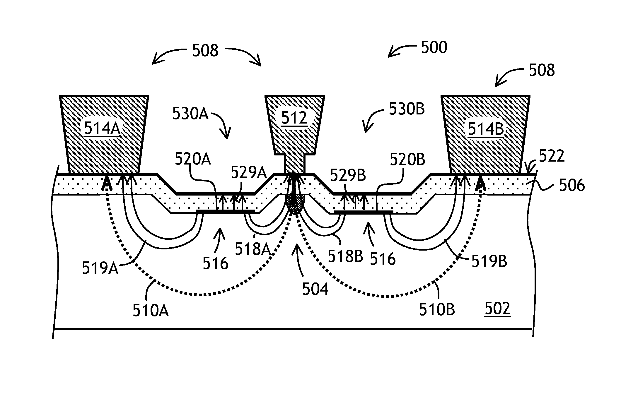
[0056]While the present teachings are described in conjunction with various embodiments and examples, it is not intended that the present teachings be limited to such embodiments. On the contrary, the present teachings encompass various alternatives, modifications and equivalents, as will be appreciated by those of skill in the art. In FIGS. 5 to 12, similar numerals refer to similar elements.

[0057]Referring to FIG. 5, an optical modulator 500, according to the present invention, includes a Z-cut electro-optical crystal substrate 502, e.g. LiNbO3 or other suitable material, having an optical waveguide 504 formed therein, a buffer layer 506 disposed over the substrate 502 in at least a partial contact with the substrate 502, an RF electrode structure 508 disposed over the buffer layer 506, and a buried bias electrode structure 516 disposed on the substrate 502 under the buffer layer 506. The RF electrode structure 508 includes a shaped RF signal electrode 512 disposed substantially p...


PUM

PropertyMeasurementUnit
thicknessaaaaaaaaaa
thicknessaaaaaaaaaa
thicknessaaaaaaaaaa

Abstract

An electro-optic device is disclosed, in which an RF signal electrode is used as a bias ground electrode. Thus, for Z-cut lithium niobate electro-optic crystals, there is no need to place a buried bias electrode under the RF signal electrode and over the optical waveguide. As a result, both optical and the RF wave propagation losses are reduced. In another embodiment, a buried bias electrode is placed over the optical waveguide between two buffer layers having a different electrical conductivity. The buffer layer underneath the buried bias electrode has a larger electrical conductivity than the buffer layer above the buried bias electrode. The buffer layer underneath the buried bias electrode reduces the optical loss penalty due to the buried bias electrode located above the optical waveguide, while the buffer layer above the bias electrode reduces leakage currents.

Description

CROSS-REFERENCE TO RELATED APPLICATIONS[0001]The present invention claims priority from U.S. provisional patent application No. 61 / 406,076, filed Oct. 22, 2010, which is incorporated herein by reference.TECHNICAL FIELD[0002]The present invention relates generally to electro-optic devices and, more specifically, to electro-optic devices used in fiberoptic telecommunications.BACKGROUND OF THE INVENTION[0003]Electro-optic devices are frequently used in fiberoptic telecommunication systems to manipulate optical signals. Frequently, these electro-optic devices include at least one optical waveguide formed from and / or in an electro-optic material. When an electric field is generated in the electro-optic material, the refractive index of the optical waveguide(s) changes, and the optical signal propagating therethrough can be altered. Some examples of common electro-optic devices used in telecommunication systems include optical modulators, optical switches, optical couplers, etc.[0004]One ...

Claims


Application Information

Patent Timeline
Patent Type & Authority Patents(United States)
IPC IPC(8): G02F1/035G02F1/03G02F1/21G02F1/225
CPCG02F1/0316Y10T29/49155G02F2001/212G02F1/2255G02F1/212
Inventor KISSA, KARLHALL, ALLEN T.
Owner LUMENTUM OPERATIONS LLC
Why Eureka
Try Eureka