Piezoelectric thin film resonator

a thin film resonator and piezoelectric technology, applied in the field of piezoelectric thin film resonators, can solve the problems of jitter characteristics of resonators or insertion loss characteristics as filters, and disturb the resonance waveform, and achieve the effect of reducing the purious resonance caused by wave propagation in the transverse direction

Inactive Publication Date: 2007-10-04
SEIKO EPSON CORP
View PDF6 Cites 17 Cited by
  • Summary
  • Abstract
  • Description
  • Claims
  • Application Information

AI Technical Summary

Benefits of technology

[0008]In accordance with an aspect of the present invention, there is provided a highly efficient piezoelectric thin film resonator in which spurious resonance caused by wave propagation in a transverse direction is reduced.
[0010]According to the piezoelectric thin film resonator, spurious due to wave propagation in a transverse direction can be reduced, and excellent jitter characteristics as a resonator or excellent insertion loss characteristics as a film can be achieved.

Problems solved by technology

In particular, when a piezoelectric thin film resonator is formed with a piezoelectric material having a high electromechanical coupling coefficient such as PZT (lead zirconate titanate), a higher harmonic component of the propagation wave in the transverse direction is superposed near the resonance frequency and the antiresonant frequency, which causes problems in that the resonance waveform is disturbed, and the jitter characteristics as a resonator or the insertion loss characteristics as a filter are deteriorated.

Method used


Image

  • Piezoelectric thin film resonator
  • Piezoelectric thin film resonator
  • Piezoelectric thin film resonator

Examples


first embodiment

1. First Embodiment

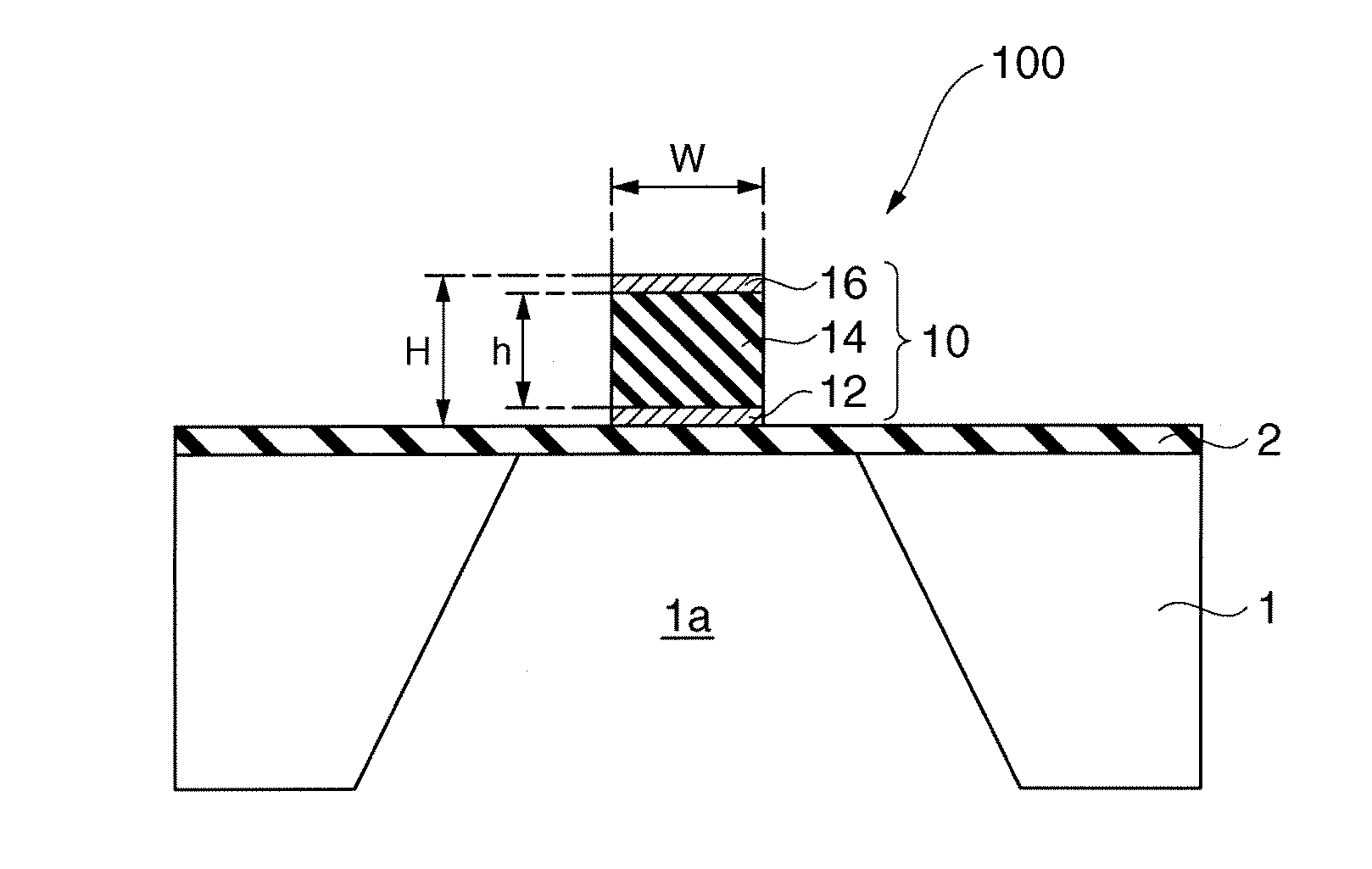
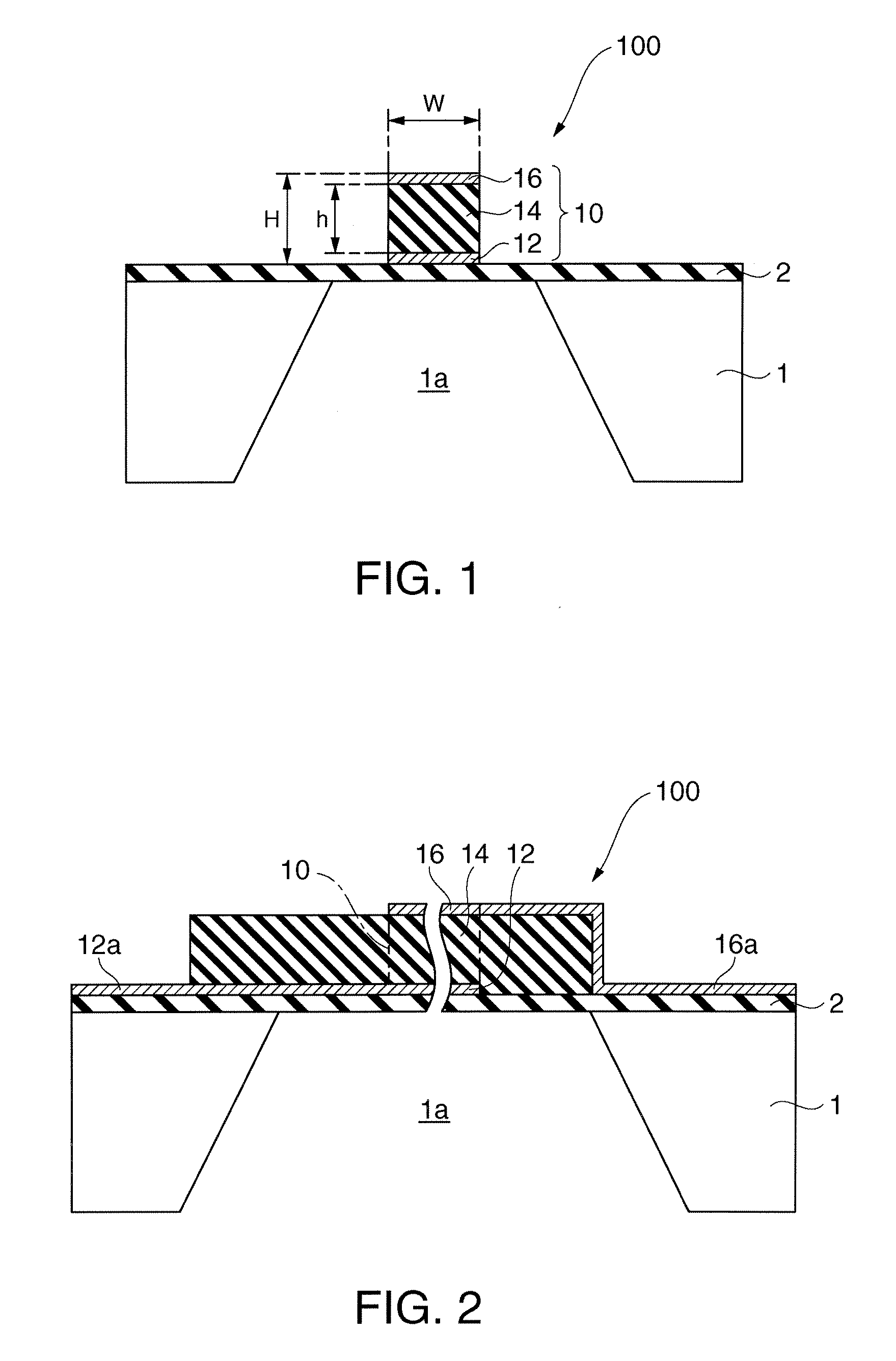
[0025]FIG. 1 is a cross-sectional view schematically showing a piezoelectric thin film resonator 100 in accordance with an embodiment of the invention. FIG. 2 is a cross-sectional view schematically showing the piezoelectric thin film resonator 100 shown in FIG. 1 in a state in which it is rotated through 90 degrees in a horizontal direction.

[0026]The piezoelectric thin film resonator 100 includes a substrate 1 and a base layer 2 formed thereon, as shown in FIG. 1 and FIG. 2. Furthermore, a resonator 10 is formed on the base layer 2.

[0027]An opening section 1a, that is called a cavity, is formed in the substrate 1. The opening section 1a is formed by etching (wet etching or dry etching) the substrate 1 from its back surface. The opening section 1a can be formed, using the base layer 2 to be described below as an etching stopper layer. By providing the opening section 1a, a mechanical restraining force to the resonator section 10 to be described below is reduced, s...

second embodiment

2. Second Embodiment

[0047]FIG. 4 is a cross-sectional view schematically showing a piezoelectric thin film resonator 200 in accordance with an embodiment of the invention. Members that are substantially the same as those of the piezoelectric thin film resonator 100 of the first embodiment shown in FIG. 1 and FIG. 2 are appended with the same reference numbers, and their detailed description is omitted. The piezoelectric thin film resonator 200 of the second embodiment has an opening section composing a free vibration region whose structure is different from that of the piezoelectric thin film resonator 100 of the first embodiment.

[0048]The piezoelectric thin film resonator 100 includes a substrate 1 and a base layer 2 formed on the substrate 1, as shown in FIG. 4. Further, a resonance section 10 is formed on the base layer 2.

[0049]An opening section 1b, that is called an air gap, is formed in the substrate 1. The opening section 1b is dug generally halfway through the substrate 1, w...

third embodiment

2. Third Embodiment

[0057]FIG. 6 is a cross-sectional view schematically showing a piezoelectric thin film resonator 300 in accordance with an embodiment of the invention. Members that are substantially the same as those of the piezoelectric thin film resonator 100 of the first embodiment shown in FIG. 1 and FIG. 2 are appended with the same reference numbers, and their detailed description is omitted. The piezoelectric thin film resonator 300 of the third embodiment has a region composing a free vibration region whose structure is different from that of the piezoelectric thin film resonator 100 of the first embodiment, and is a SMR type device.

[0058]The piezoelectric thin film resonator 300 includes a substrate 1 and an acoustic multilayer film 3 formed on the substrate 1, as shown in FIG. 6. Furthermore, a resonance section 10 is formed on the acoustic multilayer film 3. As the substrate 1, a substrate similar to the one described in the first embodiment can be used.

[0059]The acous...


PUM


Abstract

A piezoelectric thin film resonator includes a substrate, and a resonator section formed above the substrate and having a first electrode layer, a piezoelectric layer and a second electrode layer in which acoustic vibration is generated in a thickness direction of the piezoelectric layer by application of an electric field to the piezoelectric layer by the first electrode layer and the second electrode layer, wherein at least one pair of sides of a plane configuration of the resonator section are in parallel with each other, and the shortest distance in a spacing between the parallel sides in the pair is less than a thickness of at least the resonance section.

Description

[0001]The entire disclosure of Japanese Patent Application No. 2006-090253, filed Mar. 29, 2006 is expressly incorporated by reference herein.BACKGROUND[0002]1. Technical Field[0003]The present invention relates to a piezoelectric thin film resonator that uses thickness longitudinal vibration of a piezoelectric film.[0004]2. Related Art[0005]The development of communication devices such as cellular phones is trending toward an increase in frequency and a reduction in size, and for this reason, an increase in performance and a reduction in size of RF circuits are demanded. In this connection, as high frequency devices such as high frequency filters that are used in transmission / reception sections of communication devices, BAW (bulk acoustic wave) devices that can achieve the performance equivalent to that of conventional SAW (surface acoustic wave) devices, and can be more readily improved for higher frequency and reduced in size compared to SAW devices are attracting attention. The ...

Claims


Application Information

Patent Timeline
Patent Type & Authority Applications(United States)
IPC IPC(8): H01L41/00H01L41/09H01L41/18H01L41/187H01L41/22H01L41/29H03H9/17
CPCH03H3/02H03H9/02157H03H2003/021H03H9/174H03H9/175H03H9/173
Inventor HIGUCHI, TAKAMITSUFURUHATA, MAKOTO
Owner SEIKO EPSON CORP
Why Eureka
Try Eureka