Organic light-emitting diode, contact arrangement and method for producing an organic light-emitting diode

Active Publication Date: 2014-07-29
DOLYA HOLDCO 5 LTD
View PDF27 Cites 5 Cited by
  • Summary
  • Abstract
  • Description
  • Claims
  • Application Information

AI Technical Summary

Benefits of technology

[0005]It is therefore an object of the invention to provide an organic light-emitting diode and a contact arrangement for a two-dimensional, optically active element which allows improved electrical connection of a layer stack or of an optically active ele

Problems solved by technology

One problem of conventional light-emitting di

Method used


Image

  • Organic light-emitting diode, contact arrangement and method for producing an organic light-emitting diode
  • Organic light-emitting diode, contact arrangement and method for producing an organic light-emitting diode
  • Organic light-emitting diode, contact arrangement and method for producing an organic light-emitting diode

Examples


Example

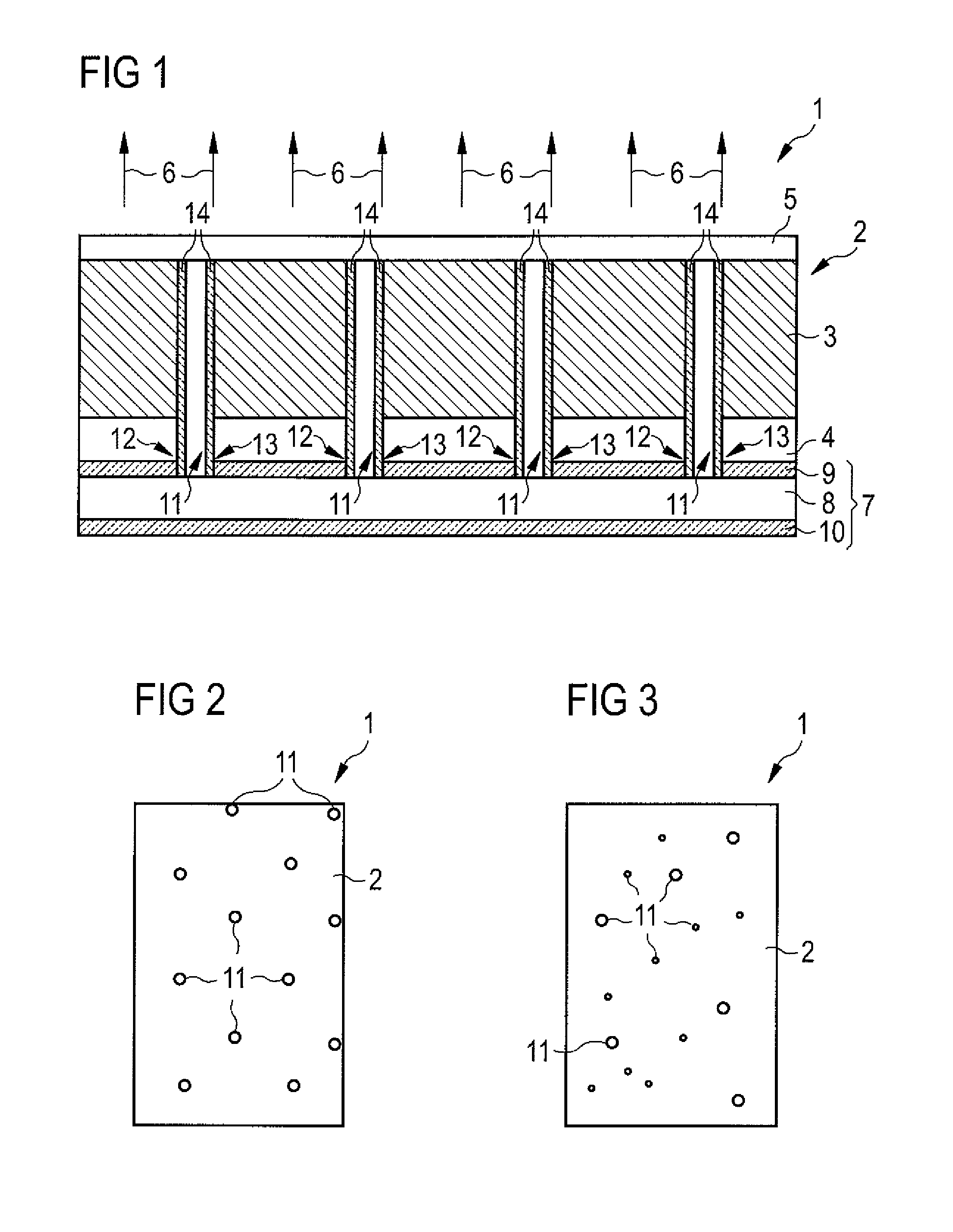
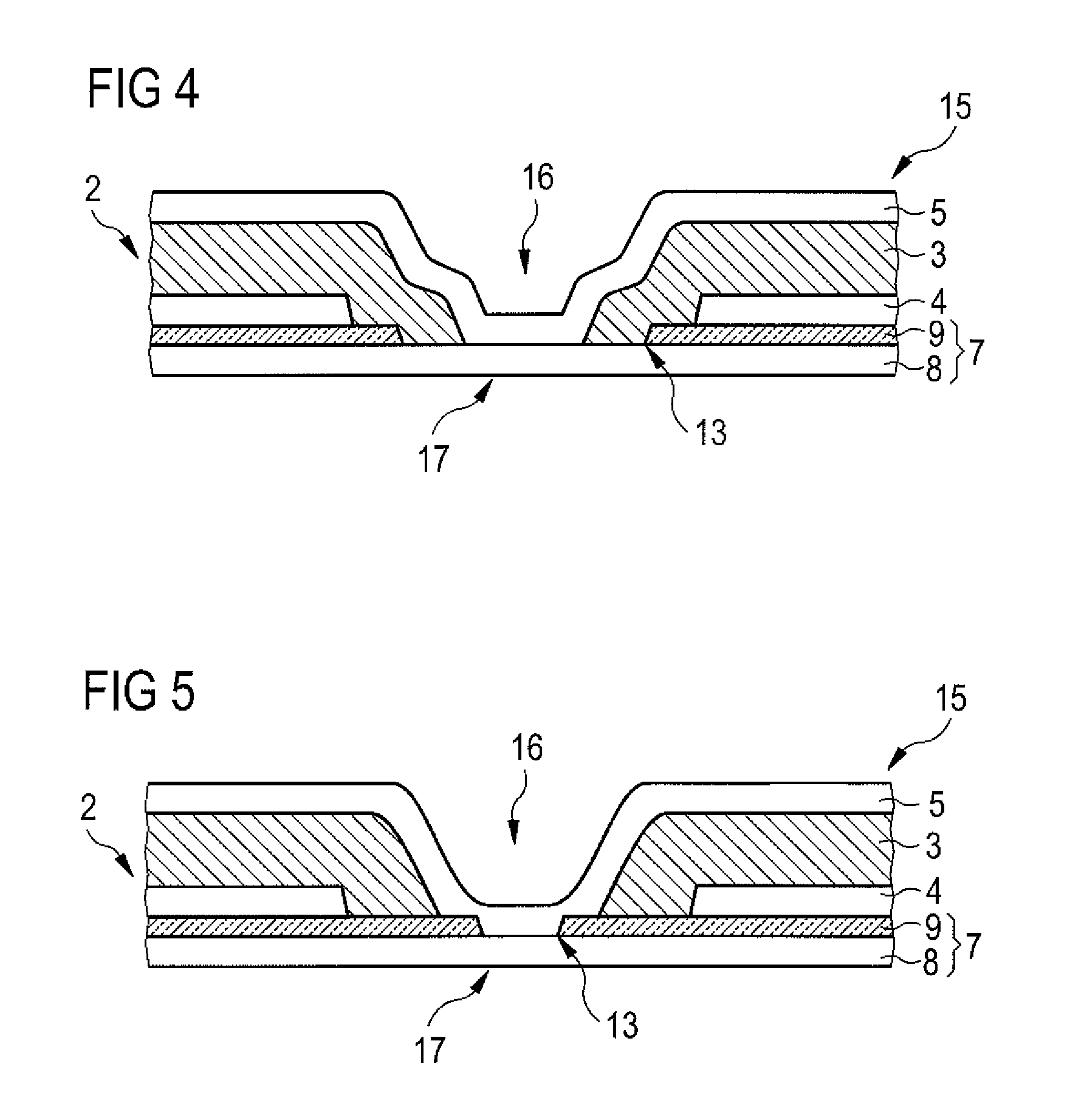
DETAILED DESCRIPTION OF THE DRAWINGS

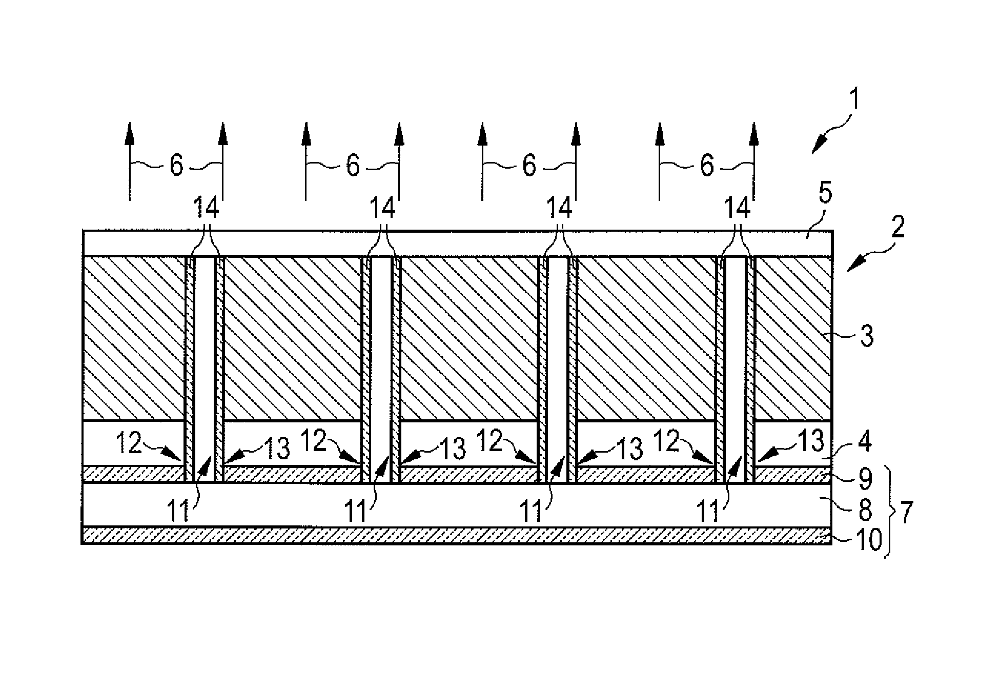
[0047]FIG. 1 shows a cross-section through an organic light-emitting diode 1 according to one exemplary embodiment. The organic light-emitting diode 1 comprises a layer stack 2, which comprises at least one organic layer 3 for emitting electromagnetic radiation. The layer stack 2 may additionally contain further organic and inorganic layers, which are necessary or advantageous for forming a diode structure. Examples of such layers are layers for hole transport or electron transport, emitter layers, n-doped layers, p-doped layers, buffer layers and intermediate layers, as are known to a person skilled in the art. For reasons of clarity, such additional layers are, however, not shown in FIG. 1.

[0048]The layer stack 2 contains a functional region with one or more functional layers of organic materials. The functional layers may here for example take the form of electron transport layers, electroluminescent layers and / or hole transport layers. In the ...


PUM


Abstract

An organic light-emitting diode (1), comprising a layer stack (2) for emitting electromagnetic radiation (6). An electrically conductive first connection layer (4) is arranged on a first surface of the layer stack (2) and an electrically conductive second connection layer (5) at least predominantly transparent to a characteristic wavelength of the emittable electromagnetic radiation (6) is arranged on a second surface of the layer stack (2). The organic light-emitting diode is characterized by a conductive contact structure (7) arranged on the opposite side of the first connection layer (4) from the layer stack, which contact structure is connected electrically to the second connection layer (5) in the region of a plurality of openings (12) in the first connection layer (4). Also disclosed is a contact arrangement (15) for a two-dimensional, optically active element and to a method of producing organic light-emitting diodes (1).

Description

RELATED APPLICATIONS[0001]This is a U.S. national stage of application No. PCT / DE2008 / 000217, filed on Feb. 16, 2009.[0002]This application claims the priority of German application no. 10 2008 011 867.2 filed Feb. 29, 2008 and 10 2008 020 816.7 filed Apr. 25, 2008, the entire content of which is hereby incorporated by reference.FIELD OF THE INVENTION[0003]The invention relates to electronic components with a two-dimensional, optically active area in general and to organic light-emitting diodes in particular. In this respect, two-dimensional means that the optically active element extends substantially further in a first and second spatial direction defining the first and second surfaces than in the remaining third spatial direction.BACKGROUND OF THE INVENTION[0004]One problem of conventional light-emitting diodes is uniform feed of an operating voltage. Conventionally the operating voltage for an organic layer stack is applied to edge areas of two connection layers. While electrica...

Claims


Application Information

Patent Timeline
IPC IPC(8): H01L33/00H01L33/32H01L33/38H01L33/48H01L33/62
CPCH01L33/62H01L33/486H01L2224/48091H01L33/32H01L33/38H01L51/5203H01L51/5212H01L51/5228H01L51/5234H01L2251/5361H01L2924/12044H10K50/805H10K50/814H10K50/824H10K50/828H01L2924/00H10K59/352H10K50/84H10K50/85
Inventor LANG, ERWINBECKER, DIRKDOBBERTIN, THOMASKLEIN, MARKUS
Owner DOLYA HOLDCO 5 LTD
Why Eureka
Try Eureka