

Printed circuit board and semiconductor package using the same
- Summary
- Abstract
- Description
- Claims
- Application Information
AI Technical Summary
Benefits of technology
Problems solved by technology
Method used
Image

Examples
Embodiment Construction
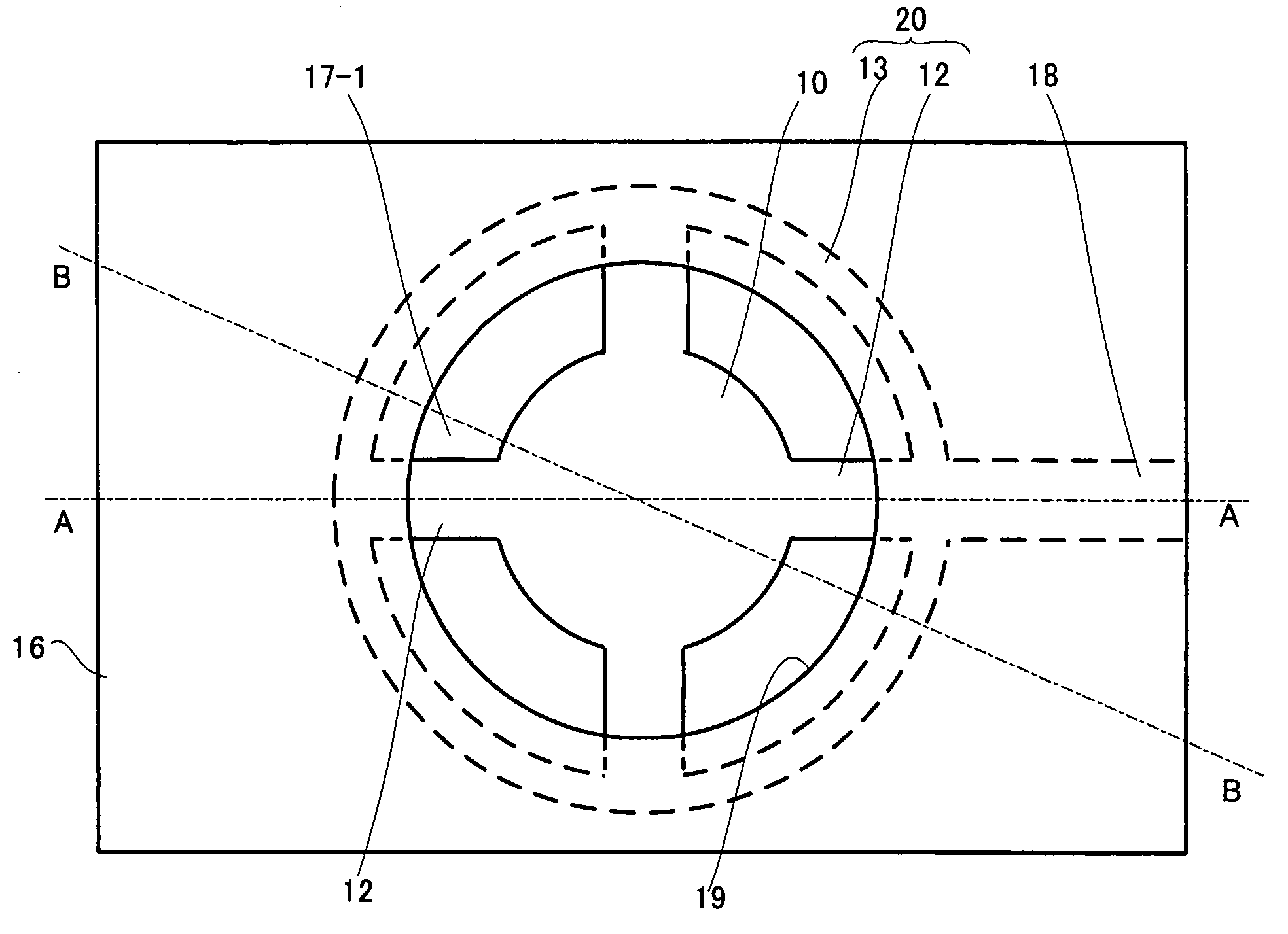
[0038]Embodiments of the present invention will be described below with reference to FIGS. 3A to 5B.
[0039]FIGS. 3A to 3C are enlarged views showing one of land areas in a printed circuit board according to a first embodiment of the present invention.
[0040]FIG. 3A is a plan view, FIG. 3B is a cross-sectional view taken along line A-A of FIG. 3A, and FIG. 3C is a cross-sectional view taken along line B-B of FIG. 3A.
[0041]As shown in FIGS. 3A to 3C, a circular land 10, a signal line 18 as part of a main wiring pattern, and an auxiliary wiring pattern 20 are formed on a surface 17-1 of an insulator printed board 17. The auxiliary wiring pattern 20 includes a first auxiliary wiring portion 13 having an annular shape and a plurality of second auxiliary wiring portions 12 each having a linear shape. The second auxiliary wiring portions 12 connect the land 10 to the first auxiliary wiring pattern 13. Specifically, the second auxiliary wiring portions 12 radially extend from the land 10 to t...
PUM
 Abstract
Description
Claims
Application Information