Ceramic multi-layer circuit substrate and manufacturing method thereof

Inactive Publication Date: 2010-03-11
SAMSUNG ELECTRO MECHANICS CO LTD
View PDF3 Cites 25 Cited by
  • Summary
  • Abstract
  • Description
  • Claims
  • Application Information

AI Technical Summary

Benefits of technology

[0017]According to exemplary embodiments of the present invention, a plurality of ceramic blocks each having a thickness 1.5 mm or less are bonded with each other using bonding green sheets having bonding electrodes in order to prevent electrode patterns from being displaced during firing. Accordingly, in the case of manufacturing a probe card, bonding pads can be accurately matched on

Problems solved by technology

In this case, however, the via-electrodes or the internal electrodes are displaced due to constriction of the ceramic green sheets

Method used


Image

  • Ceramic multi-layer circuit substrate and manufacturing method thereof
  • Ceramic multi-layer circuit substrate and manufacturing method thereof
  • Ceramic multi-layer circuit substrate and manufacturing method thereof

Examples


Embodiment Construction

[0025]The present invention will now be described more fully hereinafter with reference to the accompanying drawings, in which exemplary embodiments thereof are shown.

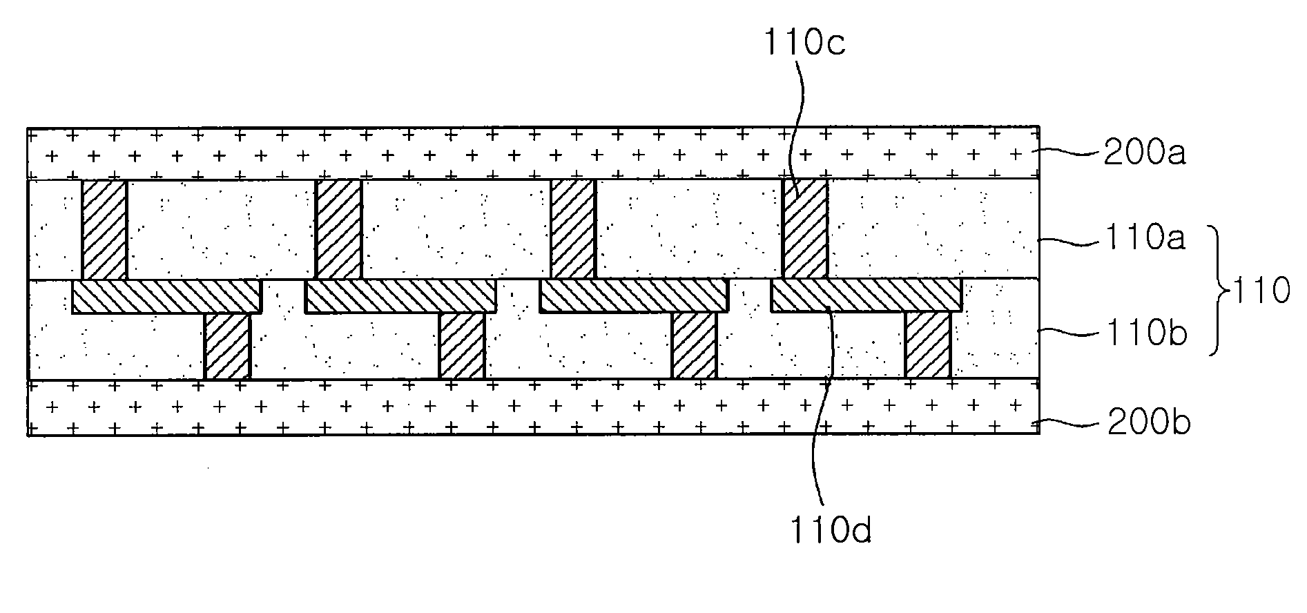
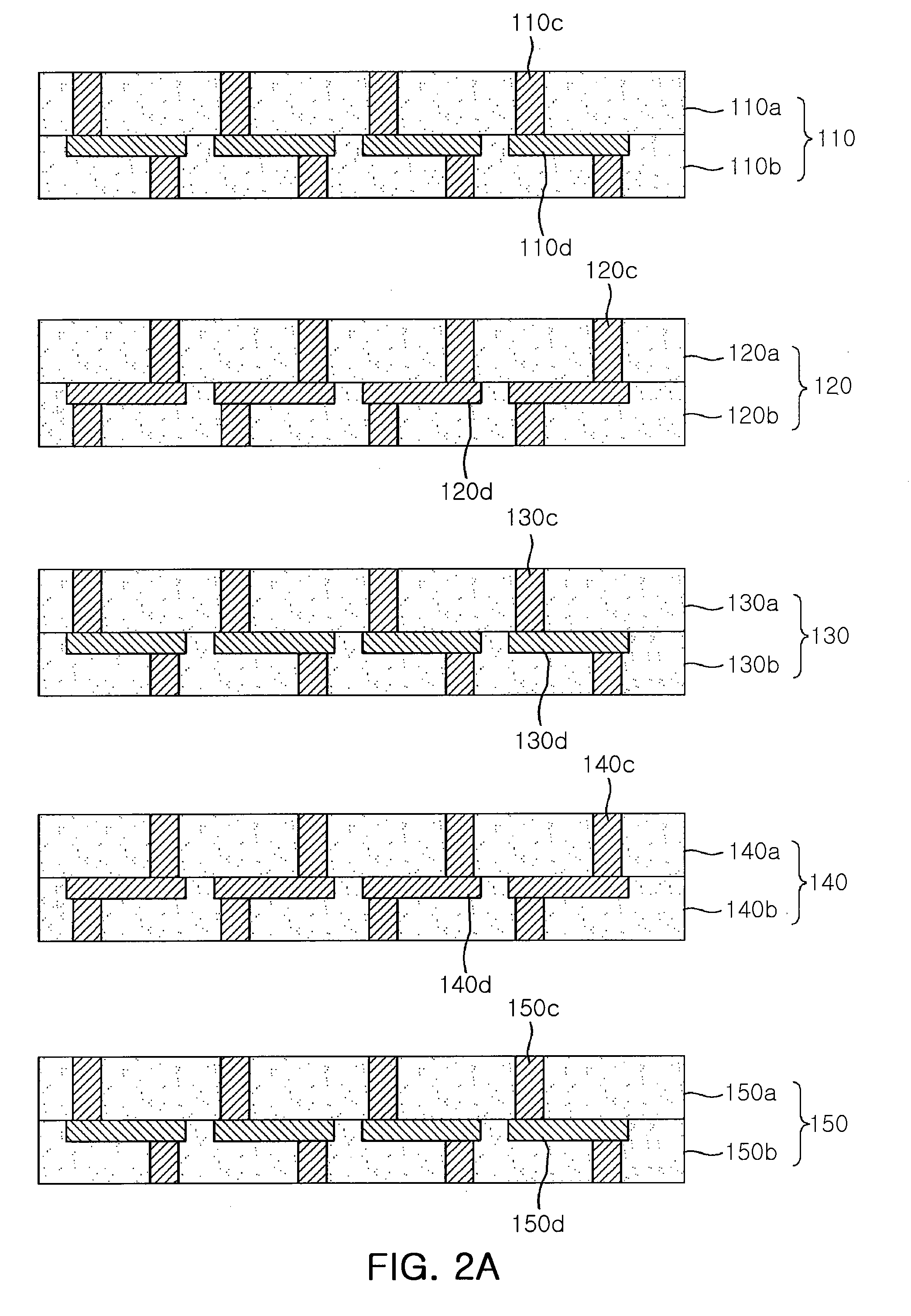
[0026]FIGS. 2A through 2D are cross-sectional views illustrating a process of manufacturing a ceramic multi-layer circuit substrate according to an exemplary embodiment of the invention. Firstly, as shown in FIG. 2A, first through fifth ceramic blocks 110,120,130,140 and 150, each of which is formed of a plurality of ceramic green sheets, are prepared.

[0027]Specifically, the first ceramic block 110 includes first and second ceramic green sheets 110a and 110b, in which via-electrodes 110c and internal electrodes 110d are formed, and the second ceramic block 120 includes third and fourth ceramic green sheets 120a and 120b, in which via-electrodes 120c and internal electrodes 120d are formed. Likewise, the third ceramic block 130 includes fifth and sixth ceramic green sheets 130a and 130b, in which via-electrodes 130c and...


PUM

PropertyMeasurementUnit
Thicknessaaaaaaaaaa
Thicknessaaaaaaaaaa
Thicknessaaaaaaaaaa

Abstract

Provided is a method of manufacturing a ceramic multi-layer circuit substrate. A plurality of ceramic blocks, in each of which one or more ceramic green sheets having via-electrodes are layered one atop the other, are formed and are then fired. The fired ceramic blocks are aligned with each other. One or more bonding green sheets each having bonding electrodes in positions corresponding to the via-electrodes of the ceramic blocks are prepared. Each of the bonding green sheets is interposed between a pair of the ceramic blocks opposing each other. The ceramic blocks and the bonding green sheets are bonded and are then fired.

Description

CROSS-REFERENCE TO RELATED APPLICATIONS[0001]This application claims the priority of Korean Patent Application No. 2008-87827 filed on Sep. 5, 2008, in the Korean Intellectual Property Office, the disclosure of which is incorporated herein by reference.BACKGROUND OF THE INVENTION[0002]1. Field of the Invention[0003]The present invention relates to a ceramic multi-layer circuit substrate and, more particularly, to a ceramic multi-layer circuit substrate used in a probe card and a manufacturing method thereof.[0004]2. Description of the Related Art[0005]A typical semiconductor test apparatus for testing electric characteristics of chips manufactured on a wafer includes a variety of constitutional parts such as a tester, a performance board, a probe card and so on. In the semiconductor test apparatus, the probe card functions to transfer a signal from the tester via the performance board to pads of the chips on the wafer and to transfer a signal from the chip pads via the performance b...

Claims


Application Information

Patent Timeline
IPC IPC(8): H05K1/11C03B25/00
CPCB32B18/00C04B2237/708C04B2237/565C04B2237/62H05K1/0306H05K3/1291H05K3/4617H05K3/4629H05K2201/0195H05K2201/096H05K2201/10378H05K2203/1126H05K2203/1476C04B37/005C04B2237/04C04B2237/32C04B2237/52C04B2237/595C04B2237/68C04B2237/704C04B2237/562H05K3/40H05K3/46
Inventor YOO, WON HEECHANG, BYEUNG GYULEE, TAEK JUNGKIM, YONG SUK
Owner SAMSUNG ELECTRO MECHANICS CO LTD
Why Eureka
Try Eureka