

Electronic apparatus and manufacturing method thereof
- Summary
- Abstract
- Description
- Claims
- Application Information
AI Technical Summary
Benefits of technology
Problems solved by technology
Method used
Image

Examples
embodiment
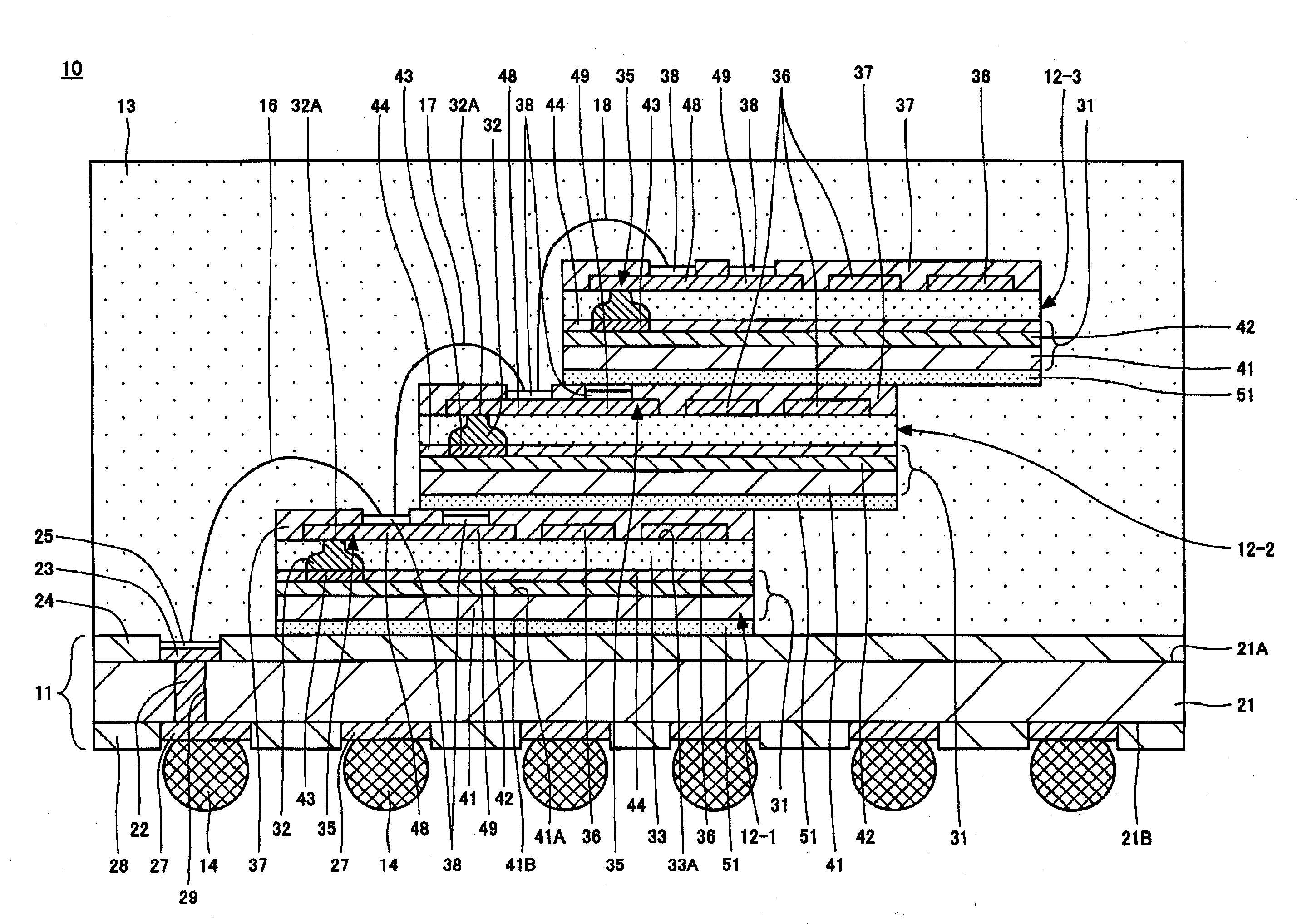
[0063]FIG. 8 is a sectional diagram of an electronic apparatus according to an embodiment of the invention.
[0064]Referring to FIG. 8, an electronic apparatus 10 of the present embodiment has a wiring substrate 11, semiconductor apparatuses 12-1 to 12-3 which are a plurality of semiconductor apparatuses, a sealing resin 13 and external connection terminals 14.
[0065]The wiring substrate 11 has a core substrate 21, a through via 22, a pad 23, solder resists 24, 28, a diffusion preventive film 25 and pads 27 for external connection. The core substrate 21 is a substrate formed in a plate shape and has a through hole 29. As a material of the core substrate 21, for example, a glass epoxy resin or an FR-4 can be used. The through via 22 is disposed in the through hole 29. The upper end of the through via 22 is connected to the pad 23 and the lower end of the through via 22 is connected to the pad 27 for external connection. The through via 22 is a via for making electrical connection betwee...
PUM
 Abstract
Description
Claims
Application Information