

Semiconductor device and method of manufacturing the same
- Summary
- Abstract
- Description
- Claims
- Application Information
AI Technical Summary
Benefits of technology
Problems solved by technology
Method used
Image

Examples
first embodiment
1. First Embodiment
[0034]1-1. Structure
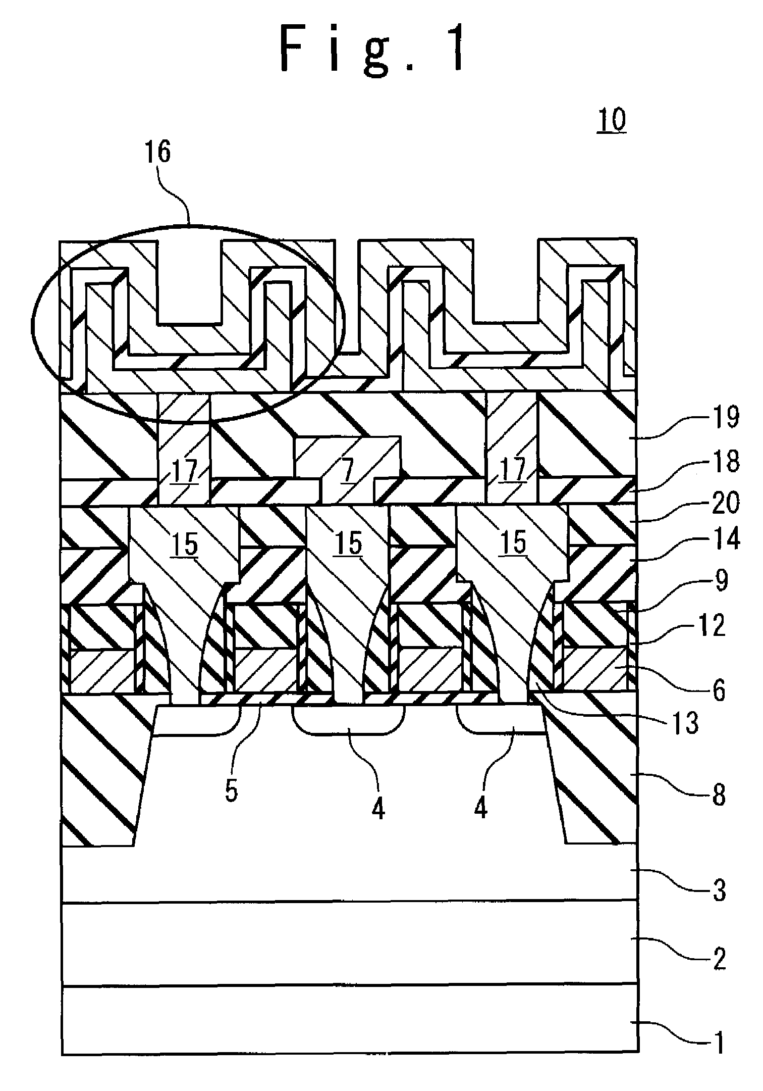
[0035]FIG. 1 is a cross-sectional view illustrating a semiconductor device 10 according to a first embodiment of the present invention. In the present embodiment, the semiconductor device 10 is exemplified by a DRAM formed on a p-type semiconductor substrate (silicon substrate) 1. Although FIG. 1 shows a cross section of a memory cell portion of the DRAM, a peripheral circuitry (not shown) is formed around the memory cell portion.
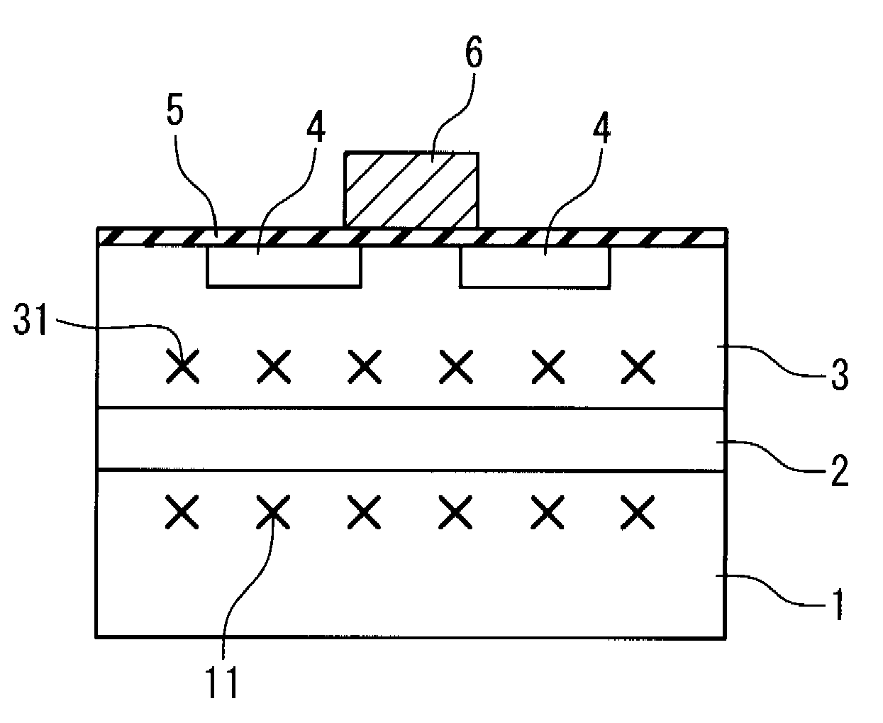
[0036]As shown in FIG. 1, a deep n-type well 2 is formed in the p-type semiconductor substrate 1. A shallow p-type well 3 is formed in the deep n-type well 2. Moreover, a memory cell transistor is formed on the shallow p-type well 3. The memory cell transistor is a MOS transistor and has n-type diffusion layers 4, a gate insulating film 5 and a gate electrode 6. The n-type diffusion layers 4 are formed in the p-type well 3 and serves as source / drain.
[0037]In FIG. 1, two memory cell transistors sharing one bit line 7 ar...
second embodiment
2. Second Embodiment
[0076]2-1. Structure
[0077]Next, a second embodiment of the present invention will be described. According to the present embodiment, a heavy metal gettering site (11, 31) is added to the semiconductor device 10, as compared with the structure in the first embodiment. In the present embodiment, the same reference numerals are given to the same components as those described in the first embodiment, and an overlapping description will be appropriately omitted.
[0078]FIG. 8 is a cross-sectional view schematically illustrating the semiconductor device 10 according to the present embodiment. Shown in FIG. 8 are the p-type semiconductor substrate 1, the deep n-type well 2, the shallow p-type well 3 and the memory cell transistor (4, 5, 6).
[0079]Under a bias condition in the normal operation, a depletion layer 28 (not shown in FIG. 8, see FIG. 9) is formed around the interface between the p-type semiconductor substrate 1 and the deep n-type well 2. A heavy metal gettering...
example-1
[0098]First, the DRAM illustrated in FIG. 1 was manufactured. Then, the bias application process (Step S21) was performed before the characteristic inspection of the wafer (Step S20: the first inspection process). As shown in FIG. 6, voltages of 2 V, 0 V, −1 V and −2 V were applied to the n-type source / drain diffusion layer 4, the shallow p-type well 3, the deep n-type well 2 and the p-type semiconductor substrate 1, respectively. That is to say, a reverse bias was applied between the n-type source / drain diffusion layer 4 and the p-type well 3, a forward bias was applied between the p-type well 3 and the n-type well 2, and a reverse bias was applied between the n-type well 2 and the p-type semiconductor substrate 1. The temperature during the bias application was set to a range from 80 to 100 degrees centigrade that are usually used in an operation test. After the bias application process, the operation test was performed (Step S20) and the yield was checked. As a result, the fracti...
PUM
 Abstract
Description
Claims
Application Information