Digital pixel addition method and device for processing plurality of images

a digital pixel addition and image processing technology, applied in the field of image processing techniques, can solve the problems of loss of resolution, image quality impairment, and drop in the signal-to-noise ratio of captured images, and achieve the effects of reducing resolution loss, high sensitivity, and high s/n ratio

Inactive Publication Date: 2014-08-26
MITSUBISHI ELECTRIC CORP
View PDF18 Cites 7 Cited by
  • Summary
  • Abstract
  • Description
  • Claims
  • Application Information

AI Technical Summary

Benefits of technology

[0007]An object of the present invention is to provide an image processing device, an image processing method, and an imaging device that can achieve both high sensitivity and a high S / N ratio under low illumination conditions and mitigate the consequent loss of resolution.
[0019]The present invention can provide both high sensitivity and a high S / N ratio under low illumination conditions, and can also mitigate the loss of resolution.

Problems solved by technology

An image signal captured in a dim environment, however, includes a comparatively large noise component, so if it is electrically amplified, or if a long exposure is made, the S / N ratio (signal-to-noise ratio) of the captured image may drop.
A problem with the proposed digital pixel addition method is that since a single pixel is generated by adding the digital signals of a number of pixels (for example, two or three pixels), resolution is lost and the image quality is impaired.

Method used


Image

  • Digital pixel addition method and device for processing plurality of images
  • Digital pixel addition method and device for processing plurality of images
  • Digital pixel addition method and device for processing plurality of images

Examples


first embodiment

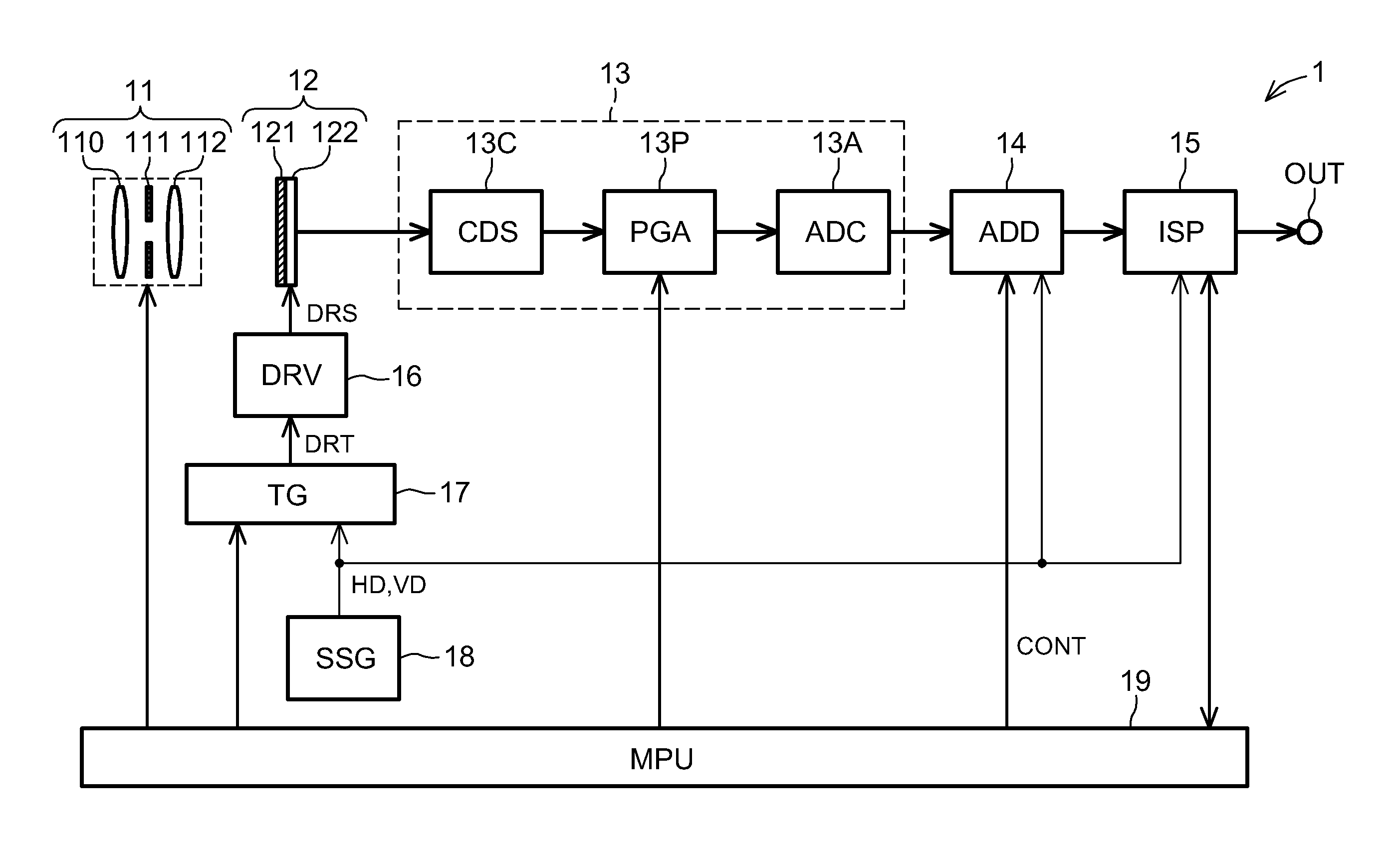
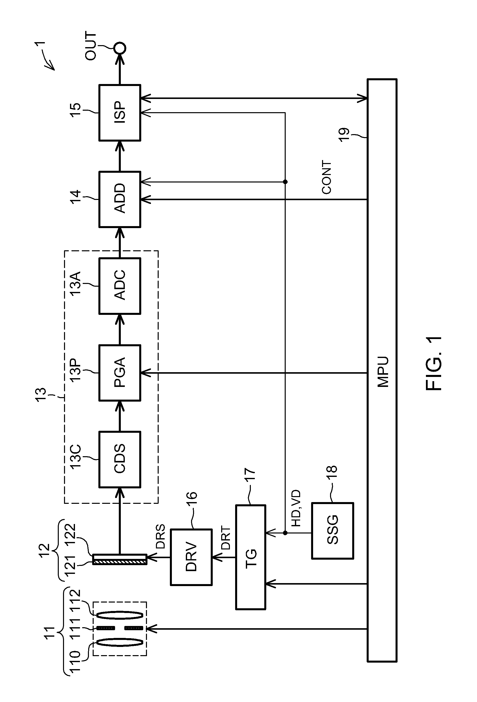
[0130]FIG. 1 is a block diagram showing the general structure of an imaging device 1 according to a first embodiment of the invention. The imaging device 1 shown in FIG. 1 has imaging optics (a lens unit) 11, a CCD image sensor 12, a front end section 13, a pixel adding circuit (image processing device) 14, an image signal processor (ISP) 15, a drive circuit (DRV) 16, a timing generator (TG) 17, a synchronization signal generator (SSG) 18, and a microprocessing unit (MPU) 19 that functions as a control unit. The imaging optics 11 include a front lens 110, a diaphragm 111, and a rear lens 112.

[0131]The CCD image sensor 12 is a single plane solid-state imager having a single color filter array 121 and a single CCD device 122. The color filter array 121 has N types of color filters (where N is an integer equal to or greater than two) arrayed in a periodic manner in a plane. These filters transmit light of colors in N mutually differing wavelength regions. The color filter array 121 use...

second embodiment

[0346]FIG. 97 is a block diagram showing the general structure of the imaging device 2 in a second embodiment of the present invention. This imaging device 2 differs from the imaging device 1 in the first embodiment in having a different MPU 19B and an additional image detection circuit 81. The second embodiment has the same effects as the first embodiment.

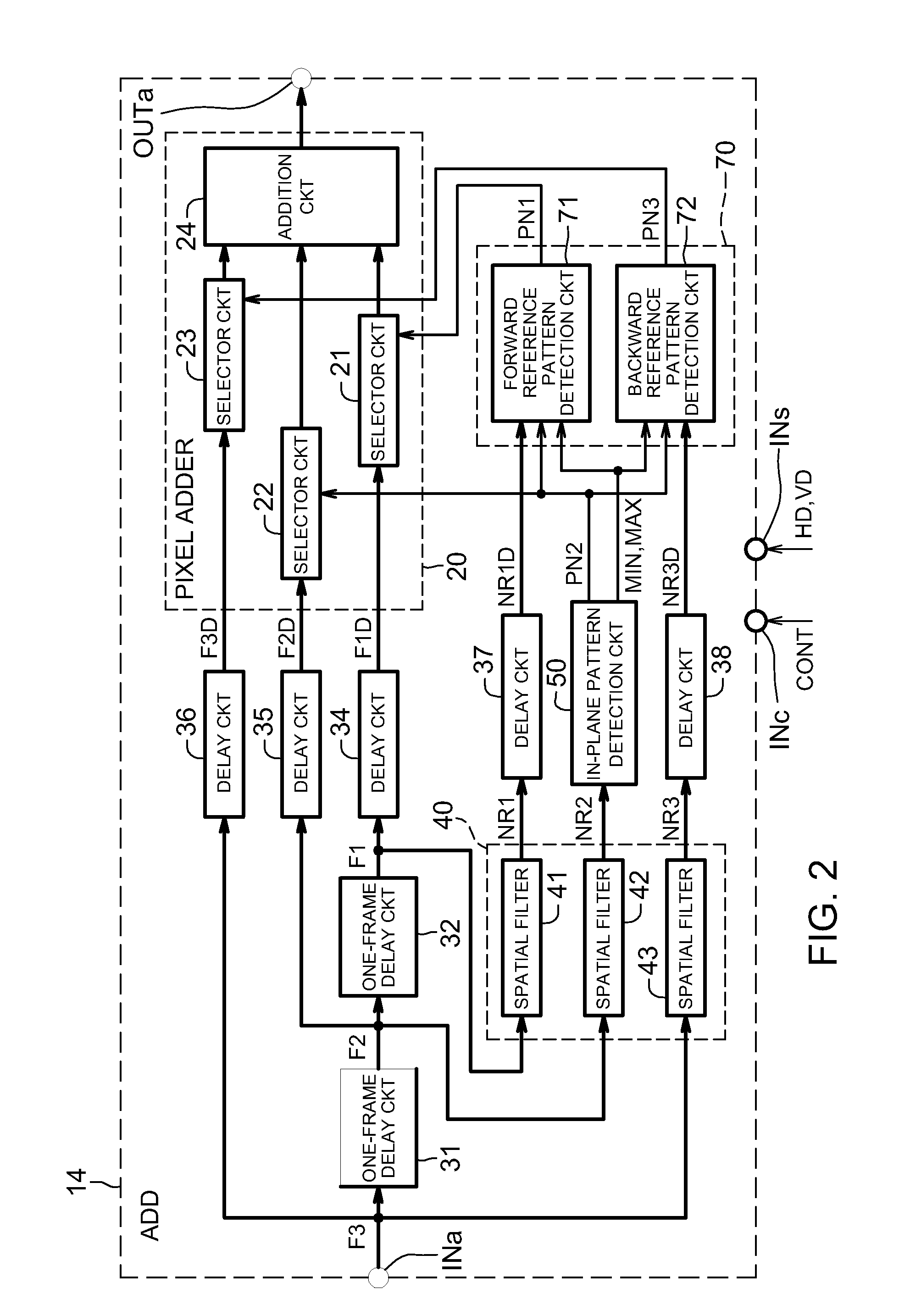
[0347]The image detection circuit 81 operates in synchronization with the horizontal synchronization signal HD and vertical synchronization signal VD supplied from the synchronization signal generator 18 and detects the luminance level or ‘speed’ of the corrected image signal output by the pixel adding circuit 14. The image detection circuit 81 has, for example, an integration function and an average level detection function. The integration function calculates an integrated value Ep by adding up the corrected pixel values in an effective pixel region included in the output signal of the pixel adding circuit 14 over a given number...

third embodiment

[0380]FIG. 99 is a block diagram showing the general structure of the imaging device 3 in a third embodiment of the present invention. This imaging device 3 differs from the imaging device 1 in the first embodiment in having a different MPU 19C and an additional light meter 82. The third embodiment has the same effects as the first embodiment.

[0381]The light meter 82 is operative to detect the subject illumination by measuring light striking the imaging surface of the CCD image sensor 12 or the imaging optics 11. The light meter 82 has an illumination sensor (not shown) that is mounted in a position determined with reference to the optical axis of the imaging optics 11.

[0382]In addition to the functions of the MPU 19 in the first embodiment, the MPU 19C has the function of controlling the exposure control parameters in accordance with the detected subject illumination value supplied from the light meter 82. More specifically, the MPU 19C can control the f-stop value of the diaphragm...


PUM


Abstract

An image processing device includes an in-plane pattern detector that selects a pixel of interest in a frame image of interest, calculates in-plane correlation index values representing correlations between the pixel of interest and in-plane pixel patterns including the pixel of interest, and selects a most highly correlated pattern as an in-plane addition pattern. A reference pattern detector calculates inter-plane correlation index values representing correlations between the in-plane pixel addition pattern and reference pixel patterns in a reference frame image temporally adjoining the frame of interest, and selects a most highly correlated reference pixel pattern. A pixel adder adds the values of the pixels in the selected in-plane pixel pattern and the selected reference pixel addition pattern to generate a corrected pixel value, thereby achieving high sensitivity and a high signal-to-noise ratio under low illumination, with little loss of resolution.

Description

BACKGROUND OF THE INVENTION[0001]1. Field of the Invention[0002]The present invention relates to image processing techniques for processing an image signal output from a solid-state imager such as a charge coupled device (CCD) image sensor or a complementary metal oxide semiconductor (CMOS) image sensor, and in particular for processing an image signal output from a solid-state imager having a color filter array.[0003]2. Description of the Related Art[0004]Digital color imaging devices such as digital still cameras and digital video cameras with CCD or CMOS image sensors are now in common use. Many of them use single plane solid-state imagers having a single image plane that receives a focused optical image through a single color filter array. A Bayer arrangement of primary colors or secondary colors is widely used in the color filter array. A Bayer array of primary colors is generally an array of red (R), green (G), and blue (B) color filters; a Bayer array of complementary colors ...

Claims


Application Information

Patent Timeline
Patent Type & Authority Patents(United States)
IPC IPC(8): G06K9/68
CPCG06K9/68H04N5/23232H04N2209/045H04N23/951
Inventor SUZUKI, DAISUKEYAMASHITA, KOICHI
Owner MITSUBISHI ELECTRIC CORP
Why Eureka
Try Eureka