Liquid crystal device and method of manufacture thereof

a liquid crystal device and liquid crystal technology, applied in the field of liquid crystal devices, can solve the problems of poor performance of the prior art polymer stabilised device (denoted by“”), dull bright state, and inability to easily be seen by the naked eye of the viewer, and achieve the effect of facilitating the stabilisation of the transient sta

Inactive Publication Date: 2014-09-09
MERCK PATENT GMBH
View PDF8 Cites 0 Cited by
  • Summary
  • Abstract
  • Description
  • Claims
  • Application Information

AI Technical Summary

Benefits of technology

[0012]The method of the present invention may also be used to stabilise states which exist for short periods of time. For example, the switched HS state in pi-cell devices may only exist for a period of several milliseconds; by the repetitive driving of the cell to the switched HS state and contemporaneously causing polymer to form, then the HS state may be stabilised.
[0049]The method of the present invention facilitates the stabilisation of the transient state so that this transient state (or a related state, which will generally be a topographically similar). Such an approach avoids having transitions between topographically different states, such transitions being undesirable.

Problems solved by technology

The performance of the prior art polymer stabilised device (denoted by“Δ”) was poor, with a dull bright state at 0V.
Such wall structures may generally be small and may not be readily visible to the naked eye of the viewer.

Method used


Image

  • Liquid crystal device and method of manufacture thereof
  • Liquid crystal device and method of manufacture thereof
  • Liquid crystal device and method of manufacture thereof

Examples


Embodiment Construction

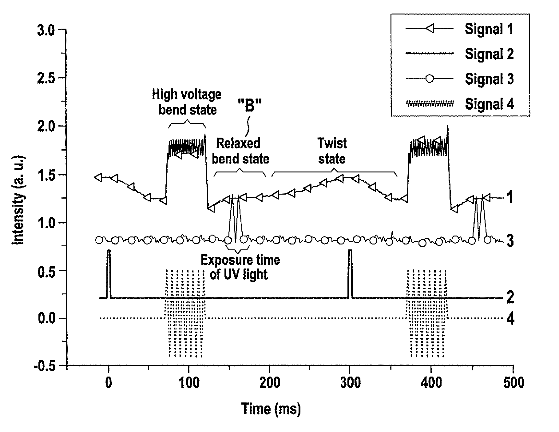
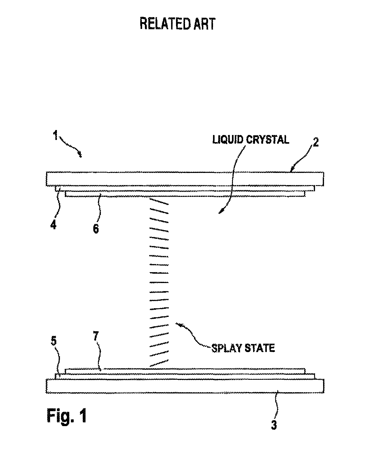
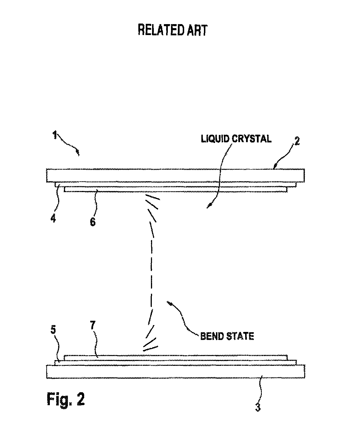
[0073]FIG. 1 is a schematic cross-section through a known liquid crystal pi cell device, the device generally denoted by reference numeral 1. The device 1 comprises parallel, transparent substrates 2, 3 (usually made of glass or plastics material), a transparent, electrically conductive layer 4, 5 on each substrate (typically indium tin oxide (ITO)) and a liquid crystal alignment surface 6, 7 applied onto each of the electrically conductive layer 4, 5. The liquid crystal alignment surface 6, 7 may be provided by a rubbed polymer, a grating or an evaporated oxide, such as silicon oxide, as will be well known to those skilled in the art. The alignment surfaces 6, 7 will cause the liquid crystal molecules in the proximity of the alignment layer to generally align in one particular direction. The liquid crystal molecules in proximity to the alignment surface do not, on average, align parallel to the surface; they are tilted with respect to the plane of the alignment surface. This tilt i...


PUM

PropertyMeasurementUnit
voltageaaaaaaaaaa
voltageaaaaaaaaaa
voltageaaaaaaaaaa

Abstract

A method of making a liquid crystal device is provided, the method comprising(i) providing a cell containing a mixture of a liquid crystal and pre-polymer(ii) applying a stimulus to arrange the liquid crystal in a first predetermined state and(iii) subsequent to, or contemporaneously with, step (ii), causing the pre-polymer to form polymer when the liquid crystal is in a second predetermined state,wherein steps (ii) and (iii) are performed a plurality of times.

Description

FIELD OF THE INVENTION[0001]The present invention relates to a liquid crystal device and a method of manufacture thereof, in particular, but not exclusively pi-cell type devices and a method of making the same.DESCRIPTION OF THE RELATED ART[0002]Many liquid crystal devices are arranged so that they may be switched (usually electrically) between two states (the two states, for example, corresponding to a dark and light state in liquid crystal displays). One state is obtained by applying a “low voltage” (possibly zero) and the second state may be obtained by applying a “high voltage” (higher than the “low voltage”. The pi cell device may be used as a display device. When a low voltage is applied to the device, the liquid crystal molecules are arranged in a highly birefringent splay state. When a high voltage is applied to the device so that the device is in a switched state, the director profile of the liquid crystal is in a bend state and the birefringence of the device is markedly l...

Claims


Application Information

Patent Timeline
Patent Type & Authority Patents(United States)
IPC IPC(8): G02F1/1333G02F1/1337C09K19/02
CPCG02F1/1395G02F2001/13775G02F1/13775
Inventor YANG, BO-RUELSTON, STEVERAYNES, PETERSHIEH, HAN-PING
Owner MERCK PATENT GMBH
Why Eureka
Try Eureka