Micro-fabricated atomic magnetometer and method of forming the magnetometer

a technology of atomic magnetometers and micro-fabricated atoms, which is applied in the field of micro-fabricated atomic magnetometers and a method of forming the magnetometer, can solve the problem of limiting the types of applications where atomic magnetometers can be commercially utilized

Active Publication Date: 2014-09-16
TEXAS INSTR INC
View PDF13 Cites 57 Cited by
  • Summary
  • Abstract
  • Description
  • Claims
  • Application Information

AI Technical Summary

Benefits of technology

[0157]As a result, the present invention significantly reduces the cost of atomic magnetometers. Another advantage of the present invention is the small size of the atomic magnetometers. Thus, the present invention allows atomic magnetometers to be incorporated into many more applications than were possible with conventional magnetometers.

Problems solved by technology

Two of the drawbacks of conventional atomic magnetometers are size and cost, which then limit the types of applications where atomic magnetometers can be commercially utilized.

Method used


Image

  • Micro-fabricated atomic magnetometer and method of forming the magnetometer
  • Micro-fabricated atomic magnetometer and method of forming the magnetometer
  • Micro-fabricated atomic magnetometer and method of forming the magnetometer

Examples


first embodiment

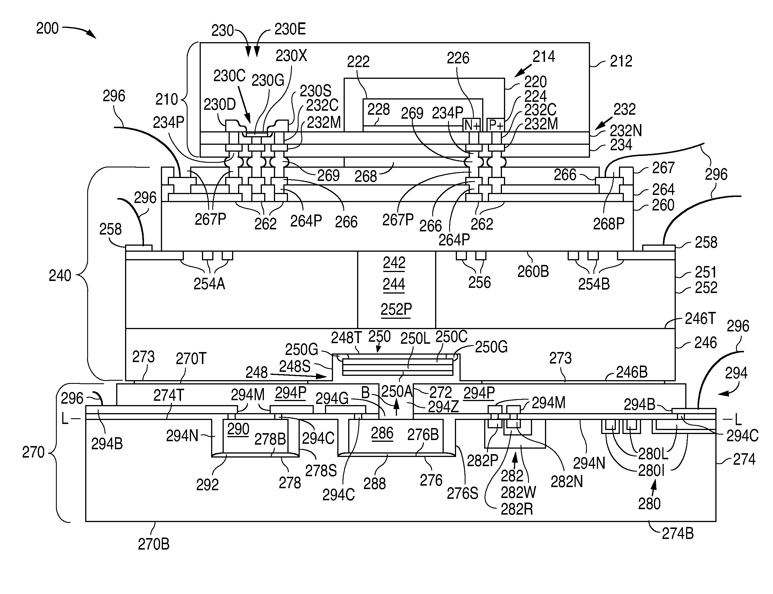
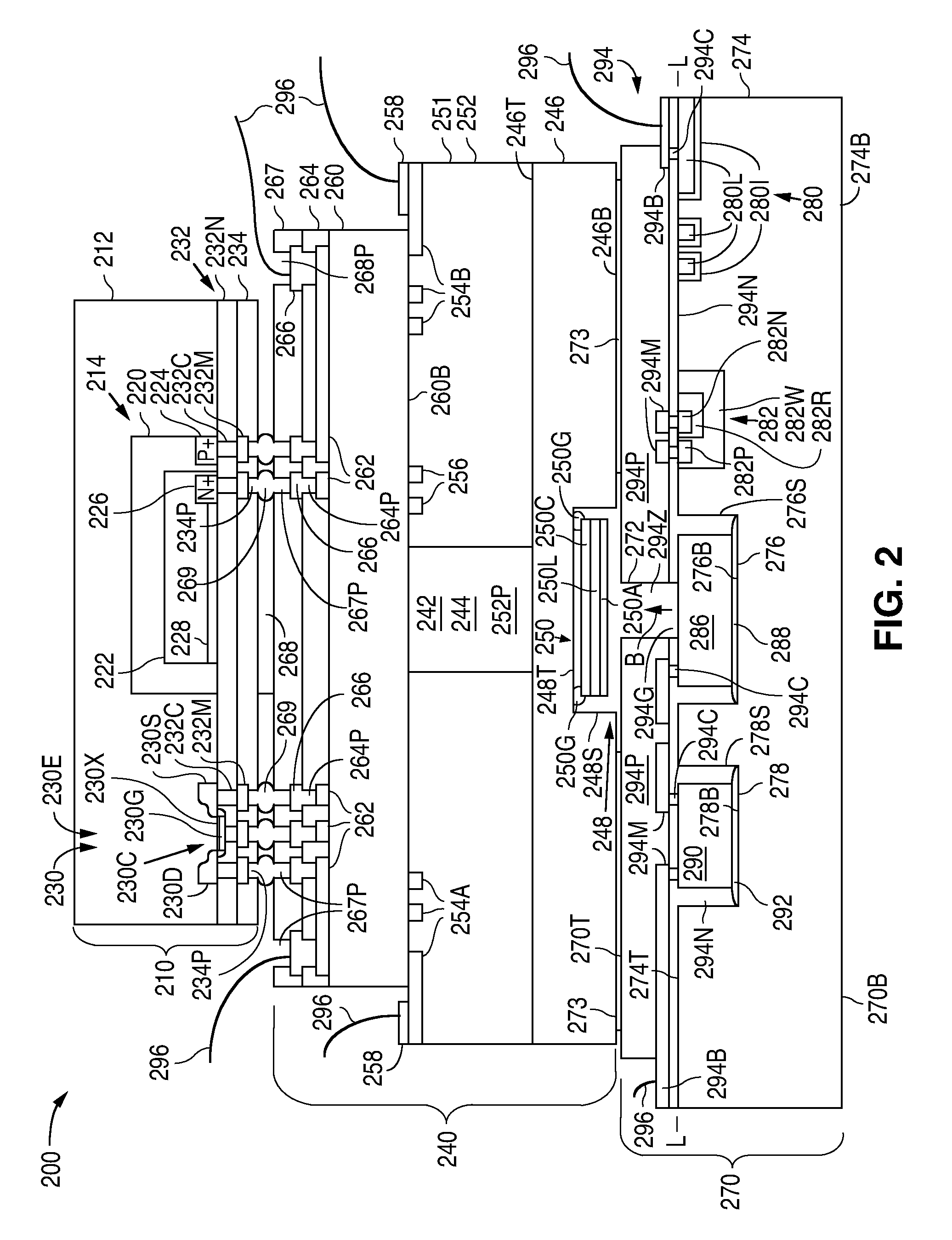
[0039]In addition, interconnect structure 232 includes a number of metal-1 structures 232M that lie on non-conductive structure 232N and touch the contacts 232C. In a first embodiment, the metal-1 structures 232M can function only as bond pad structures (locations for external electrical connections) such that an adjoining die structure provides all of the electrical interconnection required by photodiode 214 and the circuit elements 230 of electronic circuit 230E.

second embodiment

[0040]Alternately, in a second embodiment, the metal-1 structures 232M can function as bond pad structures and traces. For example, the bond pad structures can be used for power and ground, and to input signals to and output signals from electronic circuit 230E, while the traces can be used to electrically interconnect photodiode 214 and the circuit elements 230 of electronic circuit 230E. (Although interconnect structure 232 is shown with a single metal layer, additional metal layers can also be used.)

[0041]Photo detection die 210 can optionally further include a passivation layer 234 that covers non-conductive structure 232N and the metal-1 traces 232M. Passivation layer 234, which is non-conductive and moisture resistant, has a number of openings 234P that expose the pads of the metal-1 structures 232M.

[0042]As further shown in FIG. 2, atomic magnetometer 200 also includes a vapor cell die 240 that receives a light and generates the modulated light. Vapor cell die 240, which is a...


PUM


Abstract

The cost and size of an atomic magnetometer are reduced by attaching a vapor cell structure that has a vapor cell cavity to a base die that has a laser light source that outputs light to the vapor cell cavity, and attaching a photo detection die that has a photodiode to the vapor cell structure to detect light from the laser light source that passes through the vapor cell cavity.

Description

BACKGROUND OF THE INVENTION[0001]1. Field of the Invention[0002]The present invention relates to atomic magnetometers and, more particularly, to a micro-fabricated atomic magnetometer and a method of forming the magnetometer.[0003]2. Description of the Related Art[0004]An atomic magnetometer is a device that measures the strength of a magnetic field by determining a frequency known as the Larmor frequency. The Larmor frequency, in turn, is the frequency of the magnetic moment of a contained group of in-phase, spinning, outer shell electrons of alkali atoms moving in precession in response to the magnetic field. A magnetic field strength B is defined by the equation B=hvL / γ, where h is Plank's constant, hvL is the Larmor frequency, and γ is the gyromagnetic ratio (e.g., 7 Hz / nT for 87Rb and 3.5 Hz / nT for Cs).[0005]FIG. 1 shows a block diagram that illustrates an example of a prior art atomic magnetometer 100. As shown in FIG. 1, atomic magnetometer 100 includes a vertical cavity surf...

Claims


Application Information

Patent Timeline
Patent Type & Authority Patents(United States)
IPC IPC(8): G01R33/02
CPCG01R33/032H01L24/16H01L2224/131H01L2224/16145H01L2924/12042H01L2924/12043H01L2924/014H01L2924/00
Inventor FRENCH, WILLIAMLINDORFER, PHILIPPHOPPER, PETER J.PARSA, ROOZBEHWEST, ANDREW JAMESSHULVER, BYRON JON RODERICK
Owner TEXAS INSTR INC
Why Eureka
Try Eureka