Mapping of random defects in a memory device

a memory device and random defect technology, applied in the field of memory devices, can solve the problems of mram memory cells typically experiencing random defects, defects that require management, and type of defect management that is not efficien

Active Publication Date: 2014-11-11
AVALANCHE TECH
View PDF10 Cites 2 Cited by
  • Summary
  • Abstract
  • Description
  • Claims
  • Application Information

AI Technical Summary

Problems solved by technology

However, as readily known in the industry, memory arrays, which are organized in rows and columns of memory cells, readily include defective memory cells, which are generally identified prior to the memory array leaving its place of manufacturing.
Both massive as well as random defects require management if the memory array is to be used in any practical memory application.
As can be appreciated, this type of defect management is not efficient for the case of random defects because an entire row or an entire column of memory cells is likely rendered unusable even though as few as one memory cell in the row or column may be defective.
Magnetic random access memory (MRAM) is a prime candidate for having random defects due to the non-uniform etching process and other processes employed during its manufacturing, MRAM memory cells typically experience random defects as opposed to massive defects or in some cases, in addition to massive defects.
Techniques currently employed to manage random defects suffer from being costly due to their use of large memory.
As can be appreciated, the shortcoming with this technique is that a large CAM is required, causing valuable real estate in addition to increased costs to the point of being impractical.

Method used


Image

  • Mapping of random defects in a memory device
  • Mapping of random defects in a memory device
  • Mapping of random defects in a memory device

Examples


Embodiment Construction

[0020]In the following description of the embodiments, reference is made to the accompanying drawings that form a part hereof, and in which is shown by way of illustration of the specific embodiments in which the invention may be practiced. It is to be understood that other embodiments may be utilized because structural changes may be made without departing from the scope of the present invention. It should be noted that the figures discussed herein are not drawn to scale and thicknesses of lines are not indicative of actual sizes.

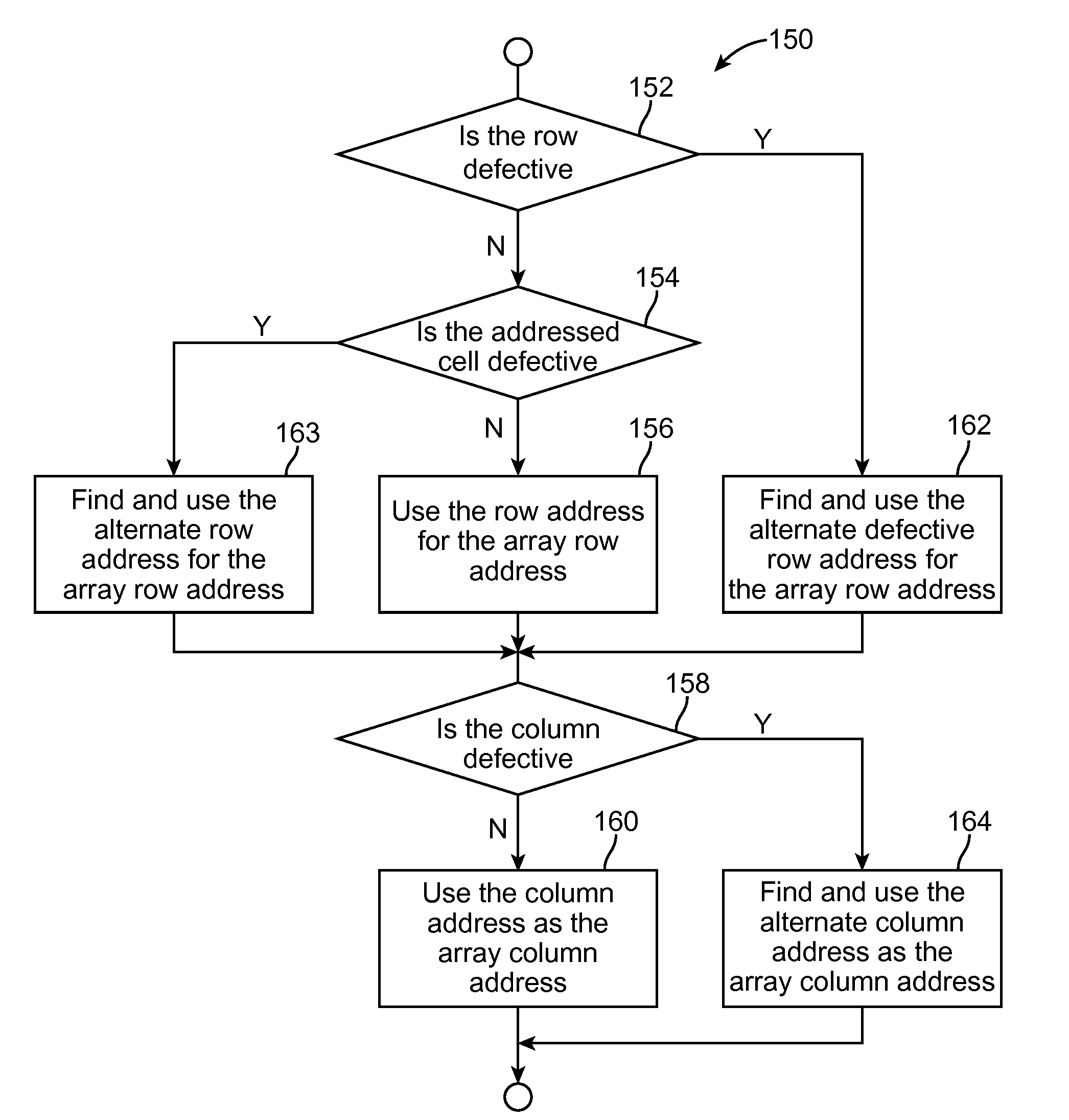
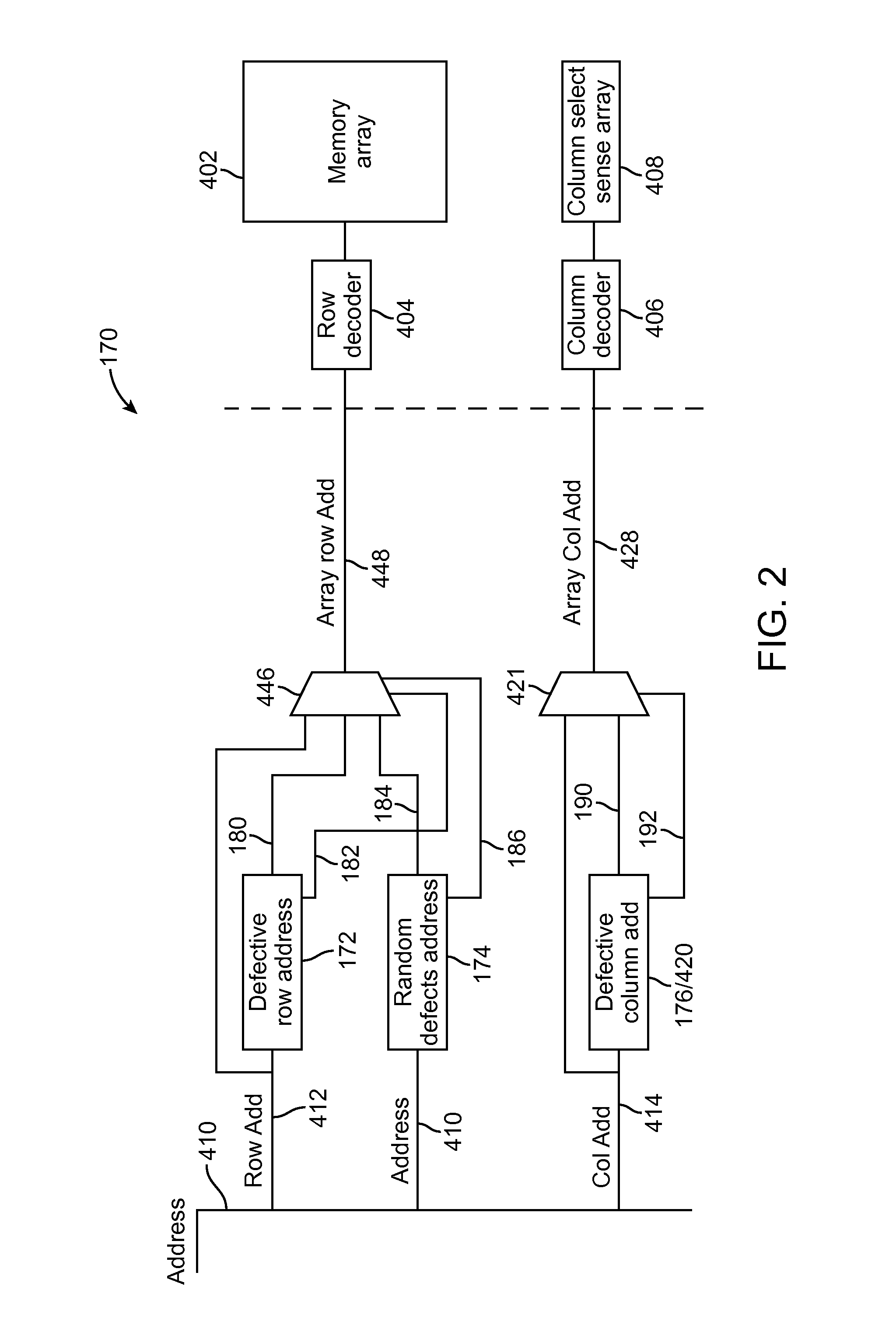
[0021]In accordance with an embodiment of the present invention, a method of managing random defects in a memory array of a memory device is disclosed. The memory array is organized into rows and columns, with a row and a column identifying a memory location identifying a memory cell. This method includes receiving an incoming address that identifies a memory location to be accessed, within a memory array. The incoming address includes a row address and a ...


PUM


Abstract

A memory device includes a memory array with random defective memory cells. The memory array is organized into rows and columns with a row and column identifying a memory location of a memory cell of the memory array. The memory device includes a row address device and a column address device and is operative to use a grouping of either the row or the column addresses to manage the random defective memory cells by mapping the memory location of a defective memory cell to an alternate memory location.

Description

BACKGROUND OF THE INVENTION[0001]1. Field of the Invention[0002]The invention relates to a memory device having a memory array and particularly to managing random defects in memory locations of the memory array of the memory device.[0003]2. Description of the Prior Art[0004]Memory arrays have a variety of applications nearly all of which require reliability of the memory locations of such arrays. However, as readily known in the industry, memory arrays, which are organized in rows and columns of memory cells, readily include defective memory cells, which are generally identified prior to the memory array leaving its place of manufacturing. These defects are characterized as “massive” defects and “random” defects. “Massive” defects generally refer to defects that render an entire row or column defective or that are greater than that which is statistically considered random defects, whereas “random” defects appear more randomly in memory cells with no particular known pattern, such as...

Claims


Application Information

Patent Timeline
Patent Type & Authority Patents(United States)
IPC IPC(8): G11C29/00
CPCG11C29/808G06F12/0684G06F2212/69G06F11/2094G06F3/0679G06F3/0619G11C29/4401G06F2212/1032G06F3/0638G11C29/72
Inventor NEMAZIE, SIAMACKABEDIFARD, EBRAHIM
Owner AVALANCHE TECH
Why Eureka
Try Eureka