
Three-dimensional (3D) hydrodynamic focusing using a microfluidic device
a microfluidic device and hydrodynamic focusing technology, applied in the field of three-dimensional (3d) hydrodynamic focusing, can solve the problems of impracticality or less accuracy, and achieve the effect of more reliable single-molecule sensitivity
- Summary
- Abstract
- Description
- Claims
- Application Information
AI Technical Summary
Benefits of technology
Problems solved by technology
Method used
Image

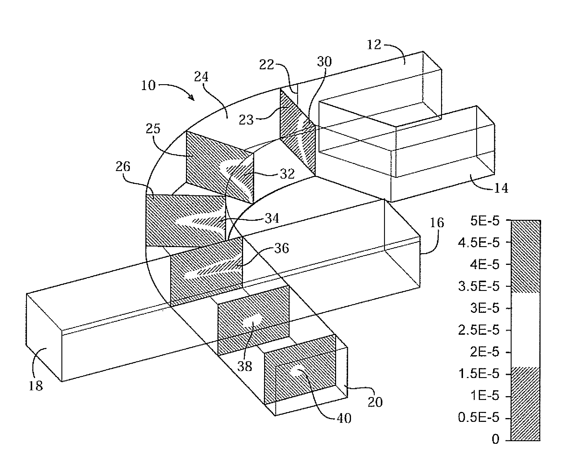
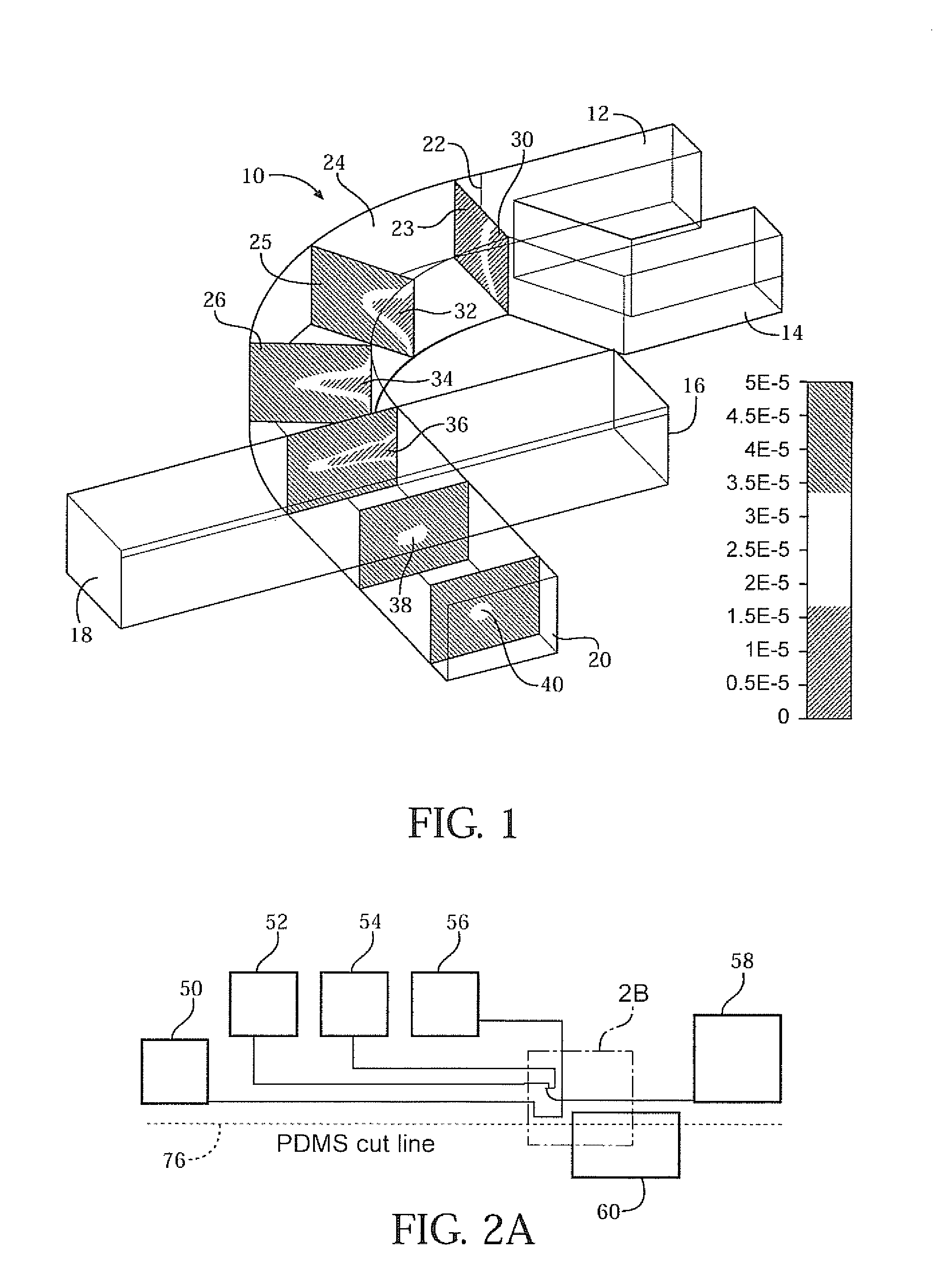
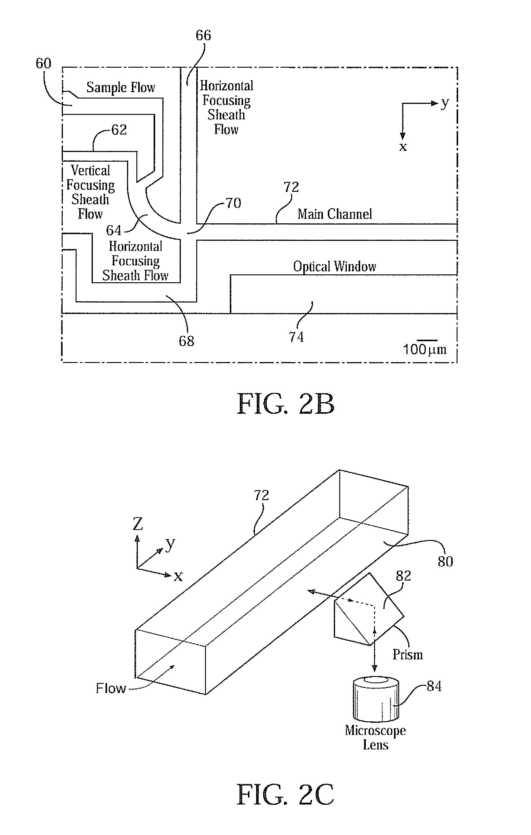
Examples
example device fabrication
[0070]Polydimethylsiloxane (PDMS) microchannels were fabricated using a standard soft lithography technique. The master mold for the soft lithography was made on a silicon wafer (TechGophers, Chino Hills, Calif.) by Deep Reactive Ion Etching (DRIE, Adixen, Hingham, Mass.). The positive photoresist Shipley 1827 (MicroChem, Newton, Mass.) was lithographically patterned on the silicon wafer to act as a mask for DRIE, and the etch depth was set at 75 μm. The final mold depth was measured using a profilometer (KLA-Tencor, San Jose, Calif.) to ensure that the desired depth had been achieved.
[0071]The silicon mold was subsequently coated with 1H,1H,2H,2H-perfluorooctyl-trichlorosilane (Sigma Aldrich, St. Louis, Mo.) after DRIE, in order to reduce surface energy and hence the damage to the PDMS channel during the demolding process. A smooth surface of the PDMS channel sidewall reduces scattering losses and improves the quality of side-view epifluorescence microscopy. Sylgard™ 184 Silicone E...
PUM
| Property | Measurement | Unit |
|---|---|---|
| bend angle | aaaaa | aaaaa |
| bend angle | aaaaa | aaaaa |
| bend angle | aaaaa | aaaaa |
Abstract
Description
Claims
Application Information