Heating element and circuit module stack structure

a technology of stack structure and heat insulating material, which is applied in the direction of heater elements, semiconductor/solid-state device details, instruments, etc., can solve the problems of releasing waste heat, unable to meet the requirements of computer design, and the inability to start up the cpu by wrapping or stuffing the computer with heat insulating materials, etc., to achieve optimal chip unit heating effect, eliminate the drawbacks of using, and facilitate spatial arrangement

Active Publication Date: 2015-06-02
ADLINK TECH INC
View PDF9 Cites 1 Cited by
  • Summary
  • Abstract
  • Description
  • Claims
  • Application Information

AI Technical Summary

Benefits of technology

[0009]The present invention has been accomplished under the circumstances in view. It is one object of the present invention to provide a heating element and circuit module stack structure, which automatically turns on an electrical heating element to heat the chip unit of the circuit module when the temperature drops below 0° C., and automatically turns off the electrically heating element when the temperature reaches a predetermined normal operating temperature range, enabling the computer providing the heating element and circuit module stack structure to be used in a low temperature or cold outdoor environment.
[0011]Further, the thermal insulation component effectively isolates the electric heating element from the thermally conductive base member of the heat sink, avoiding interfering with the functioning of the stack structure to heat the chip unit to the optimal operating condition. Thus, the heating element and circuit module stack structure effectively solves the wrapping problem and the problem of limited temperature-maintaining effects of using heat insulating materials, and effectively eliminates the drawbacks of using a resistance heating circuit or wide temperature components that are complicated and expensive to manufacture and their installation can affect the circuit layout. The application of the heating element and circuit module stack structure facilitates spatial arrangement and achieves optimal chip unit heating effects.

Problems solved by technology

However, during operation of a computer, the CPU, graphic processor and other components of the computer will release waste heat.
However, using a computer under a severe weather condition where the temperature and moisture changes in an extremely wide range, or in a desert, snow place or any other place where there is a large temperature difference between day and night or the weather is extremely cold, the computer may be unable to start up the CPU.
However, because it is the market trend to create computers having light, thin, short and small characteristics, wrapping or stuffing a computer with heat insulating materials cannot meet this computer design requirements.
Further, because a computer has many connectors and buttons, the use of heat insulating materials cannot fully protect the computer internal components against outside cold air.
However, because the circuit board carries a large amount of electronic components that are densely installed in the circuit board, it is complicated to install the heating layer in the insulating layers and metal circuit layer of the circuit board, leading to increase in manufacturing cost.
However, the installation of the MOSFETs complicates the spatial arrangement of the circuit board.
In the circuit board, the electronic components at the circuit board that are disposed close to the MOSFETs receive better heating effects, however, the electronic components at the circuit board that are disposed far from the MOSFETs cannot receive optimal heating effects.
Further, the use of the MOSFETs and the dynamic resistance controller greatly increases the cost of the heating module.

Method used


Image

  • Heating element and circuit module stack structure
  • Heating element and circuit module stack structure
  • Heating element and circuit module stack structure

Examples


Embodiment Construction

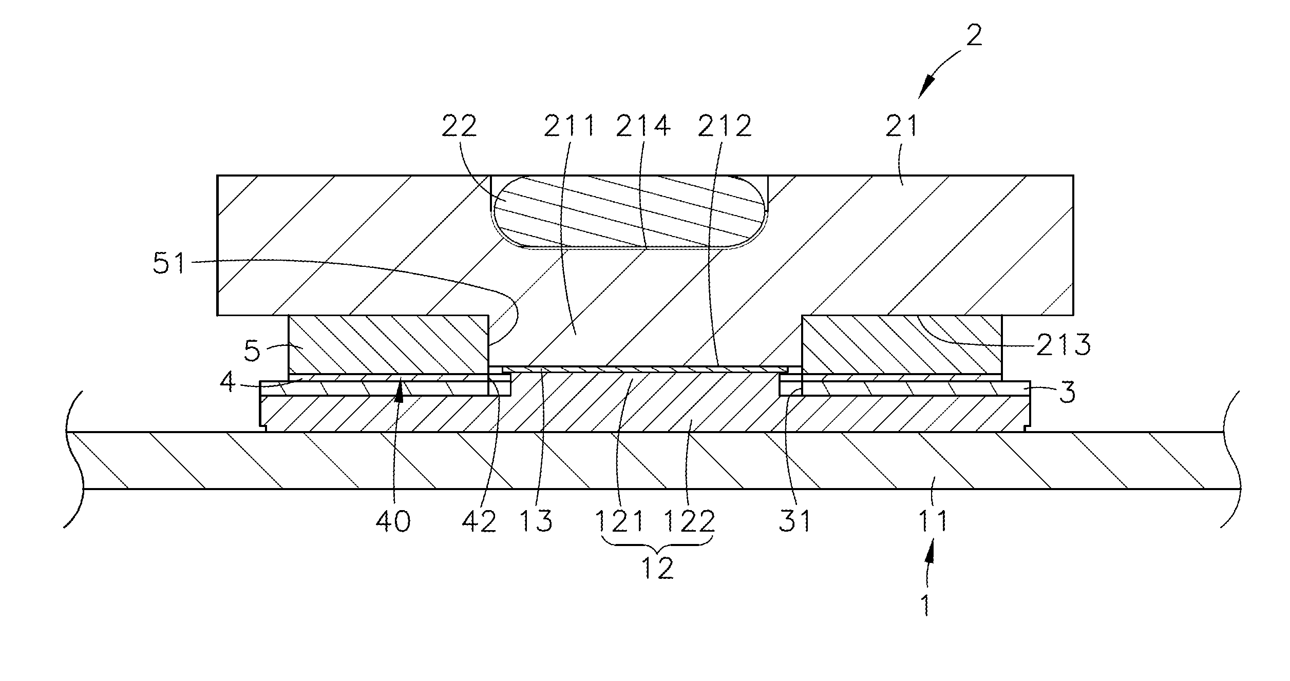
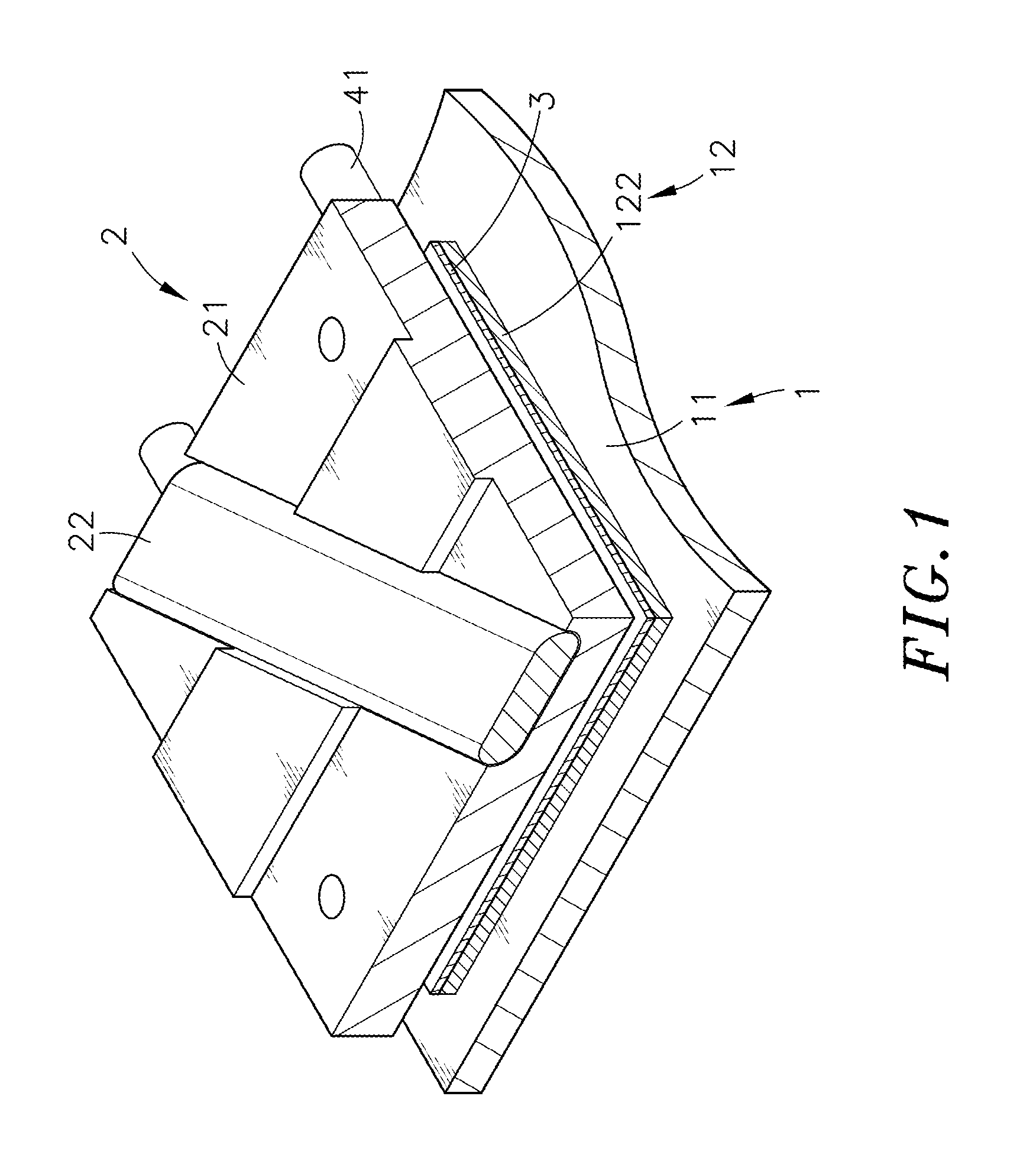
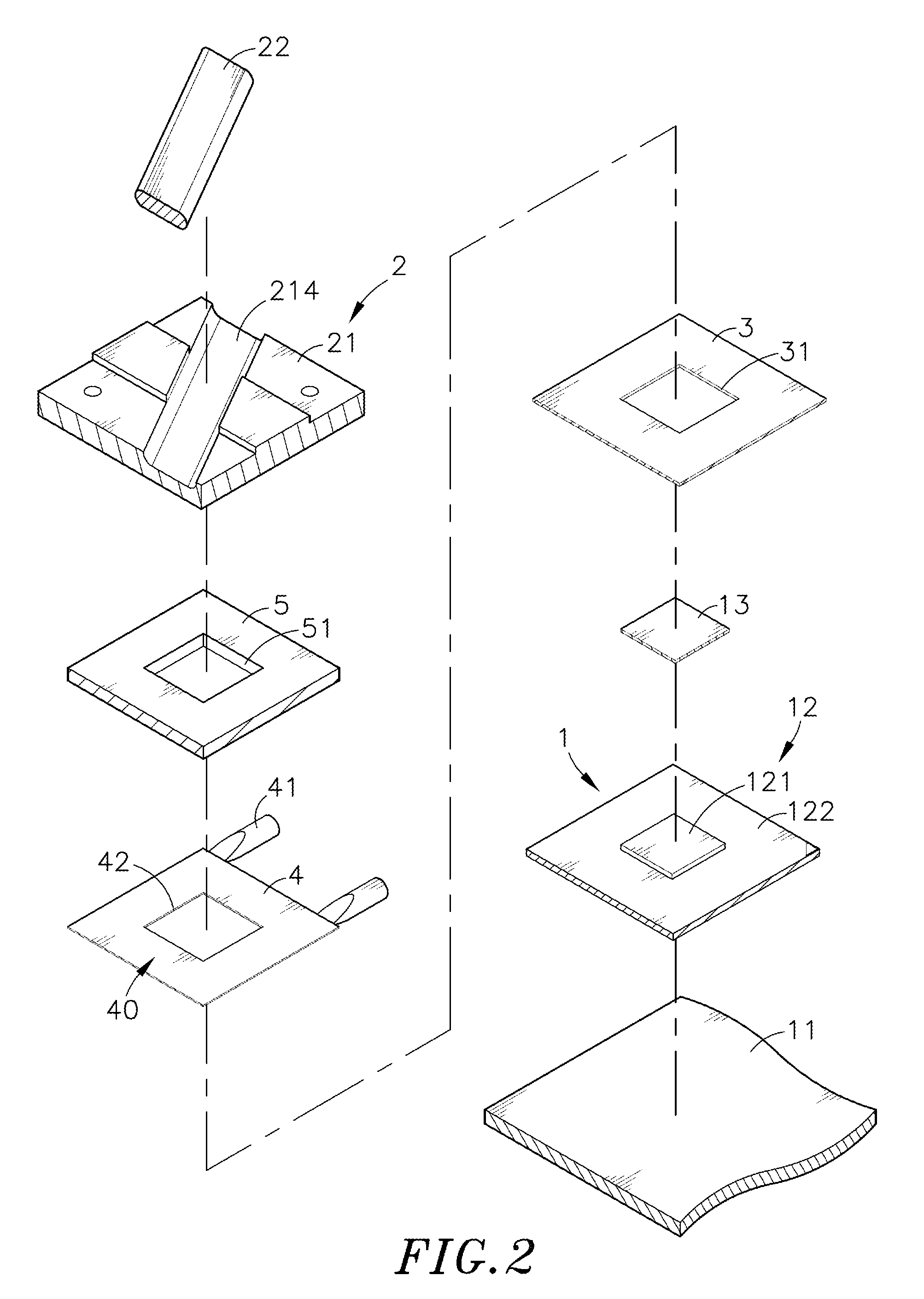
[0020]Referring to FIGS. 1-4, a heating element and circuit module stack structure in accordance with a first embodiment of the present invention is shown. As illustrated, the heating element and circuit module stack structure comprises a circuit module 1, a heat sink 2, a heat transfer layer 3, an electric heating element 4, and a thermal insulation component 5.

[0021]The circuit module 1 comprises a circuit board 11, and a chip unit 12 mounted at the top side of the circuit board 11. The chip unit 12 has its one side bonded to the circuit board 11, and its other side kept in close contact with a thermally conductive base member 21 of the heat sink 2. The thermally conductive base member 21 of the heat sink 2 has a bottom wall 213, and a flat bottom block 211 protruded from a center area of the bottom wall 213 and kept in close contact with the chip unit 12. The heat transfer layer 3 is mounted in between the bottom wall 213 of the thermally conductive base member 21 of the heat sin...


PUM


Abstract

A heating element and circuit module stack structure includes a circuit module carrying a chip unit, a heat sink having a flat bottom block protruded from a thermally conductive base member and in contact with the chip unit, a heat transfer layer set between the thermally conductive base member and the chip unit around the flat bottom block, an electric heating element mounted in between the heat transfer layer and the thermally conductive base member around the flat bottom block for heating the chip unit, and a thermal insulation component isolating the thermally conductive base member from the electric heating element. The circuit module turns on the electrical heating element when the temperature of the chip unit drops blow 0° C., and turns off the electrical heating element when the temperature reaches the normal operating temperature range, enabling the computer to be used in a low temperature or cold outdoor environment.

Description

BACKGROUND OF THE INVENTION[0001]1. Field of the Invention[0002]The present invention relates to circuit module heating technology, and more particularly to a heating element and circuit module stack structure that automatically turns on an electrical heating element to heat the chip unit of the circuit module when the temperature of the chip unit drops below 0° C. under a cold weather environment, and automatically turns off the electrical heating element when the temperature reaches a predetermined normal operating temperature range.[0003]2. Description of the Related Art[0004]Following fast development of computer electronic technology, desk computers, notebook computers, and other related products with high power, high operation speed, large capacity and low profile characteristics have been continuously created. However, during operation of a computer, the CPU, graphic processor and other components of the computer will release waste heat. An electronic component having a relat...

Claims


Application Information

Patent Timeline
Patent Type & Authority Patents(United States)
IPC IPC(8): H05B1/00H05B3/06H05B1/02H05B3/50H05B11/00H05B3/00G06F1/18H01L23/34
CPCG06F1/18H01L23/345H01L23/427H01L2924/0002G06F1/20H01L2924/00
Inventor CHIU, FANG-YUCHOU, CHUN-HUNG
Owner ADLINK TECH INC
Why Eureka
Try Eureka