
ESD clamping transistor with switchable clamping modes of operation

a technology of esd clamping transistor and switchable clamping modes, which is applied in the direction of emergency protective circuit arrangements, emergency protective arrangements for limiting excess voltage/current, electrical equipment, etc., can solve the problems of increasing capacitance, damage to electronic devices that utilize integrated circuits, etc., to achieve large ballasting resistance, high cost and printed circuit board area, and large ballasting resistance

Active Publication Date: 2015-06-09
QUALCOMM INC
View PDF11 Cites 3 Cited by
  • Summary
  • Abstract
  • Description
  • Claims
  • Application Information

AI Technical Summary

Benefits of technology

[0004]According to certain conventional techniques, an electronic device may include off-chip electrostatic discharge (ESD) protection circuits that are external to an integrated circuit. Because such off-chip protection circuits may be associated with higher cost and printed circuit board area, some integrated circuits may include ESD protection on-chip, such as using a snapback transistor clamp that utilizes a parasitic bipolar effect to dissipate current during an ESD event. However, the snapback transistor clamp may be associated with a large ballasting resistance. The large ballasting resistance may occupy significant circuit area and may increase capacitance associated with the snapback transistor clamp.

Problems solved by technology

ESD can severely alter operation of the integrated circuit or cause damage to the integrated circuit (e.g., by damaging gate oxide layers of transistors of the integrated circuit), thereby damaging an electronic device that utilizes the integrated circuit.
Because such off-chip protection circuits may be associated with higher cost and printed circuit board area, some integrated circuits may include ESD protection on-chip, such as using a snapback transistor clamp that utilizes a parasitic bipolar effect to dissipate current during an ESD event.
The large ballasting resistance may occupy significant circuit area and may increase capacitance associated with the snapback transistor clamp.

Method used


Image

  • ESD clamping transistor with switchable clamping modes of operation
  • ESD clamping transistor with switchable clamping modes of operation
  • ESD clamping transistor with switchable clamping modes of operation

Examples


Embodiment Construction

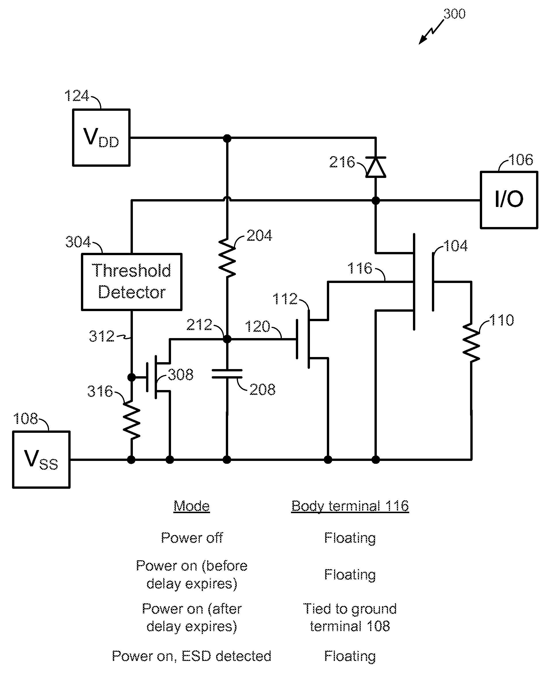
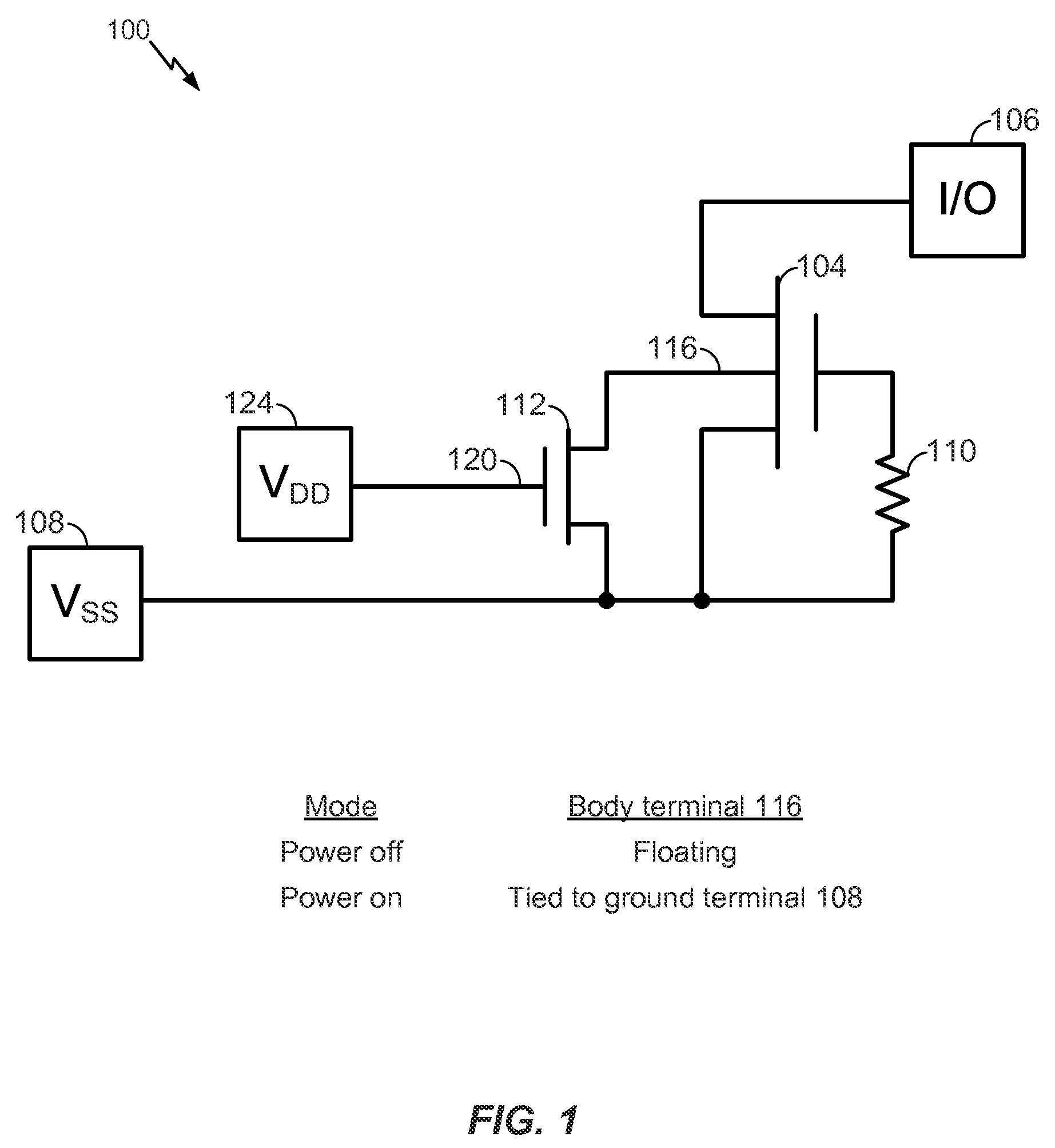
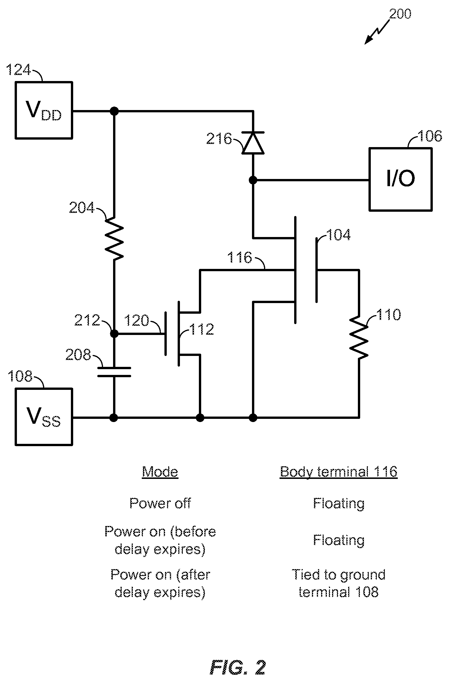
[0018]Referring to FIG. 1, a particular embodiment of a device (e.g., a semiconductor device, such as a portion of an integrated circuit) is depicted and generally designated 100. The device 100 includes an electrostatic discharge (ESD) clamping transistor 104 (e.g., a “snapback” ESD clamping transistor) coupled to a ground terminal 108 (illustrated as “VSS” in the example of FIG. 1). The ground terminal 108 may be a node of the device 100 that is biased according to a low or zero voltage.

[0019]The ESD clamping transistor 104 includes a body terminal 116. In a particular embodiment, the ESD clamping transistor 104 is compliant with one or more standards promulgated by the International Electrotechnical Commission (IEC), the Joint Electron Devices Engineering Council (JEDEC), the American National Standards Institute (ANSI), the ESD Association (ESDA), or a combination thereof. As described further below, the ESD clamping transistor 104 may have a triple-well configuration and may be...


PUM


Abstract

In a particular embodiment, an apparatus includes an electrostatic discharge (ESD) clamping transistor coupled to a ground terminal of a device. The apparatus further includes a switch coupled between a body terminal of the ESD clamping transistor and the around terminal.

Description

I. FIELD[0001]The present disclosure is generally related to electronic devices and more particularly to electronic devices that include electrostatic discharge (ESD) protection circuitry.II. DESCRIPTION OF RELATED ART[0002]Advances in technology have resulted in smaller and more powerful computing devices. For example, there currently exist a variety of portable personal computing devices, including wireless computing devices, such as portable wireless telephones, personal digital assistants (PDAs), and paging devices that are small, lightweight, and easily carried by users. More specifically, portable wireless telephones, such as cellular telephones and internet protocol (IP) telephones, can communicate voice and data packets over wireless networks. Further, many such wireless telephones include other types of devices that are incorporated therein. For example, a wireless telephone can also include a digital still camera, a digital video camera, a digital recorder, and an audio fi...

Claims


Application Information

Patent Timeline
Patent Type & Authority Patents(United States)
IPC IPC(8): H02H9/00H02H9/04
CPCH02H9/046
Inventor WORLEY, EUGENE R.WANG, MINGLIANGSRIVASTAVA, ANKITSHI, SONG S.
Owner QUALCOMM INC
Learn More