Capacitive touch panel structure

a capacitive touch panel and structure technology, applied in the field of capacitive touch panel structure, can solve the problems of compromising part of the display effect, difficult to reduce the thickness of the capacitive touch panel, and inability to meet the needs of users, so as to reduce the complexity of the fabrication process

Active Publication Date: 2015-07-14
CHENFENG OPTRONICS CORP
View PDF3 Cites 1 Cited by
  • Summary
  • Abstract
  • Description
  • Claims
  • Application Information

AI Technical Summary

Benefits of technology

[0006]The primary object of the present invention is to solve the thickness problem of the touch panel and to reduce complexity of fabrication process.
[0007]Another object of the invention is to solve the problems of lower production yield and production efficiency and higher production cost.
[0010]1. The touch control electrode is directly grown on the cover board without the need of adding an extra glass substrate, hence the thickness of the touch panel can be reduced.
[0011]2. The touch control electrode is formed on the cover board rather than embedded inside the display module, thus fabrication difficulty can be lower and production yield can be higher.
[0012]3. The display module and the touch detection module can be fabricated simultaneously and separately without being made layer by layer sequentially as the conventional techniques do, hence production efficiency can be improved.
[0013]4. As the display module and the touch detection module also are brought into production yield tests separately, in the event that the display module or the touch detection module is tested broken, replacement can be made directly, thus solving the problems of conventional techniques that have to be tested after all fabrication processes have been completed and the entire set thereof has to be discarded when defects are found. Therefore, total production yield can be higher and production cost can be lower.

Problems solved by technology

As nowadays the requirement for thin and light electronic products prevails, the difficulty in reducing the thickness of the touch panels has become the biggest issue in the industry.
However, the touch sensor occupies a portion of the display area, thus a part of the display effect is compromised.
Moreover, fabrication process of in-cell touch panels is complex and production yield enhancement is difficult.
While this prior art does not have a reduced display area, disposing the touch control module inside the liquid crystal panel still complicates fabrication process and lowers production yield.
However, as the on-cell touch panel has to be fabricated layer by layer, it is time-consuming and results in slow production speed.
Therefore, the total production yield lowers and production cost increases.
In addition, as the thinner substrates cannot withstand high temperature processes during fabrication, the electrode of the touch control module 306 is hard to be fabricated onto the second substrate 305, thereby increasing the difficulty of the production process.

Method used


Image

  • Capacitive touch panel structure
  • Capacitive touch panel structure
  • Capacitive touch panel structure

Examples


Embodiment Construction

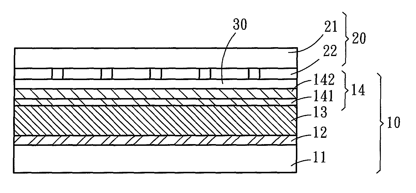
[0024]Please refer to FIGS. 3A and 3B, the present invention provides a capacitive touch panel structure which comprises a display module 10, a touch detection module 20 and an optical adhesive layer 30. The display module 10 includes a base substrate 11, a transistor layer 12, a liquid crystal layer 13 and a filter set 14 that are sequentially stacked, wherein the filter set 14 is located on the liquid crystal layer 13. In this embodiment a liquid crystal panel serves as the display module for discussion, but this is not the limitation of the invention. The base substrate 11 can be made of glass. The filter set 14 includes a color filter layer 141 which is adjacent to the liquid crystal layer 13 or the base substrate 11, and a polarization layer 142 which is connected to the color filter layer 141 and is remote from the liquid crystal layer 13 or the base substrate 11. The color filter layer 141 includes light permeable zones with three primary colors: red, blue and green. Through ...


PUM


Abstract

A capacitive touch panel structure comprises a display module, a touch detection module and an optical adhesive layer interposed between the display module and the touch detection module. The display module includes a base substrate, a transistor layer and a filter set that are sequentially stacked, namely the filter set is located on the transistor layer. The touch detection module includes a cover board and at least one touch control electrode grown on the surface of the cover board. The touch control electrode is directly formed on the surface of the cover board, hence the thickness of the capacitive touch panel of the invention can be reduced. The display module and touch detection module are made separately and bonded together via the optical adhesive layer, hence fabrication difficulty is lower and production yield is higher. Thus production speed and productivity are increased, thereby reducing production cost.

Description

FIELD OF THE INVENTION[0001]The present invention relates to a touch panel and particularly to a capacitive touch panel structure.BACKGROUND OF THE INVENTION[0002]Arising of touch control technology has revolutionized portable electronic products. Referring to FIG. 1A, a conventional out-cell capacitive touch panel comprises a screen set 1 and a touch control set 2. The screen set 1 includes a first substrate 101, a transistor layer 102, a liquid crystal layer 103, a color filter layer 104, a second substrate 105 and a polarization layer 106 that are sequentially stacked. The touch control set 2 includes a third substrate 201, a touch control module 202 and a cover glass 4 that are sequentially stacked. Also referring to FIG. 1B, the touch control module 202 further includes a first electrode 202a, an isolation layer 202b, a second electrode 202c and a hard cover layer 202d that are sequentially stacked over the third substrate 201. The first electrode 202a and the second electrode ...

Claims


Application Information

Patent Timeline
Patent Type & Authority Patents(United States)
IPC IPC(8): G06F3/044
CPCG06F3/044G06F2203/04103G06F3/0443
Inventor WONG, CHING FANG
Owner CHENFENG OPTRONICS CORP
Why Eureka
Try Eureka