Thin film transistor structure and display device having same
a thin film transistor and display device technology, applied in the field of display devices, can solve the problems of abnormal display of epd, current leakage occurring in the island structure, etc., and achieve the effect of minimizing the irradiation effect, reducing leakage current, and avoiding abnormal display of display devices
- Summary
- Abstract
- Description
- Claims
- Application Information
AI Technical Summary
Benefits of technology
Problems solved by technology
Method used
Image
Examples
first embodiment
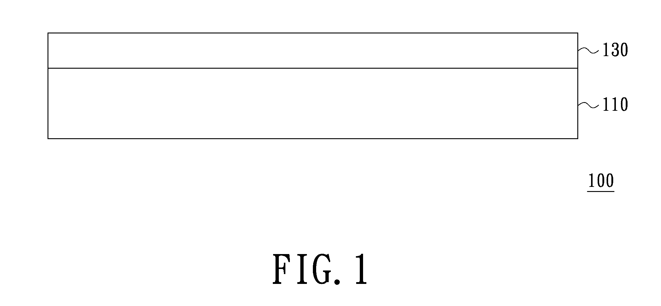
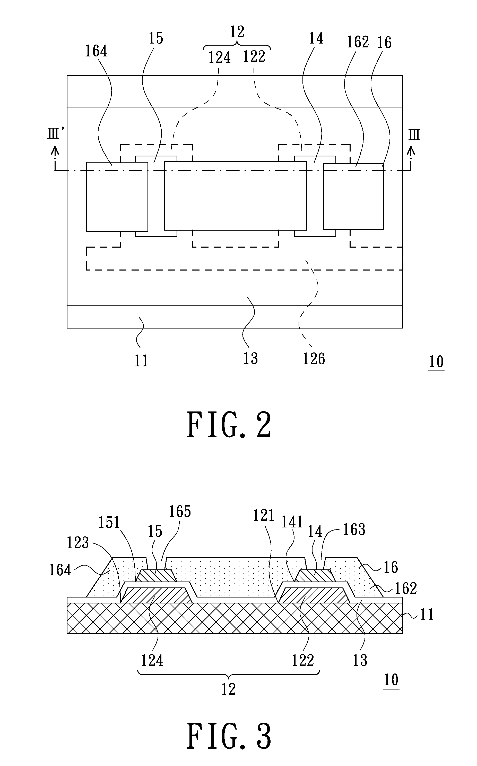
[0024]FIG. 1 schematically illustrates relative layers of a display device. FIG. 2 is a schematic top view illustrating a thin film transistor structure of the display device shown in FIG. 1. FIG. 3 is a schematic cross-sectional view taken along a line III-III′ of the thin film transistor structure shown in FIG. 2. Referring to FIG. 1, a display device 100 includes a thin film transistor (TFT) substrate 110 and a display layer 130. The display layer 130 is disposed on the TFT substrate 110.
[0025]The display device 100 is, for example, but not limited to, an electronic paper display device. In this embodiment, the display layer 130 can be an electrophoretic display layer.
[0026]Referring to FIGS. 2 and 3, the TFT substrate 110 includes a plurality of TFT structures 10. Each of the TFT structures 10 includes a substrate 11, a gate layer 12, a gate insulator layer 13, a first semiconductor island 14 serving as a first channel island, a second semiconductor island 15 serving as a second...
second embodiment
[0029]Please refer to FIG. 4 and FIG. 5, in which a TFT structure is schematically illustrated, and FIG. 5 is a schematic cross-sectional view taken along a line V-V′ of FIG. 4. In this embodiment, a TFT structure 20 includes a first semiconductor island 24 and a second semiconductor island 25, both of which have an “island out” structure. That is, opposite lateral sides 240 of the first semiconductor island 24 are outward offset from corresponding lateral sides 221 of the first gate electrode 222. The first semiconductor island 24 includes a central portion 243, a circumferential portion 242 and a bending portion 241 disposed between the central portion 243 and the circumferential portion 242, and having a turning corner. With the bending portion 241, the circumferential portion 242 deflects from the central portion 243 and extends downwards to surround the first gate electrode 222. For minimizing the area of the island, the bending portion 241 may be arranged substantially right a...
third embodiment
[0030]FIG. 6 is a schematic top view of a TFT structure in accordance with the present invention, and FIG. 7 is a schematic cross-sectional view taken along a line VII-VII′ of FIG. 6. Referring to FIGS. 6 and 7, a TFT structure 30 includes a first semiconductor island 34 having an “island in” structure and a second semiconductor island 35 having an “island out” structure, as described above.
PUM
 Abstract
Description
Claims
Application Information


