Thin film transistor substrate and display device having same

a thin film transistor and substrate technology, applied in transistors, thermoelectric devices, solid-state devices, etc., can solve problems such as abnormal display of epd and current leakage in channel islands, and achieve the effects of preventing current leakage, improving display quality of display devices, and avoiding abnormal display of display devices

Active Publication Date: 2015-10-01
E INK HLDG INC
View PDF7 Cites 5 Cited by
  • Summary
  • Abstract
  • Description
  • Claims
  • Application Information

AI Technical Summary

Benefits of technology

[0013]The above-described TFT substrates as well as the display device include any of the TFT structures include dual channel islands, thereby preventing current leakage caused by external light. As a result, the abnormal displaying of the display device can be avoided and it is helpful to improve the display quality of the display device.

Problems solved by technology

However, if the TFT structure is used in an EPD, the channel island might become conductive after being irradiated by external light, which resulting in current leakage occurring in the channel island.
As a result of the current leakage, the EPD suffers from abnormal displaying (e.g. image or color distortion).

Method used


Image

  • Thin film transistor substrate and display device having same
  • Thin film transistor substrate and display device having same
  • Thin film transistor substrate and display device having same

Examples


first embodiment

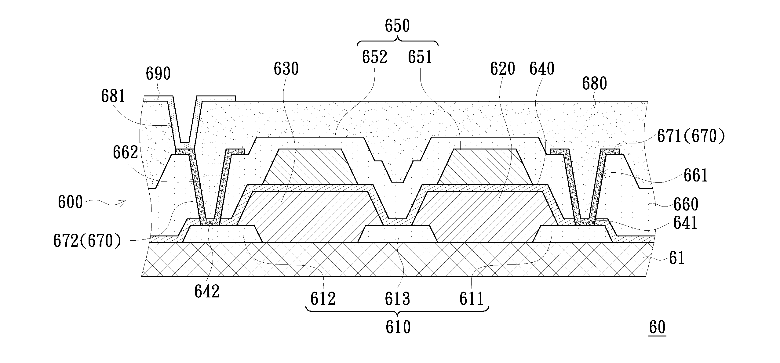
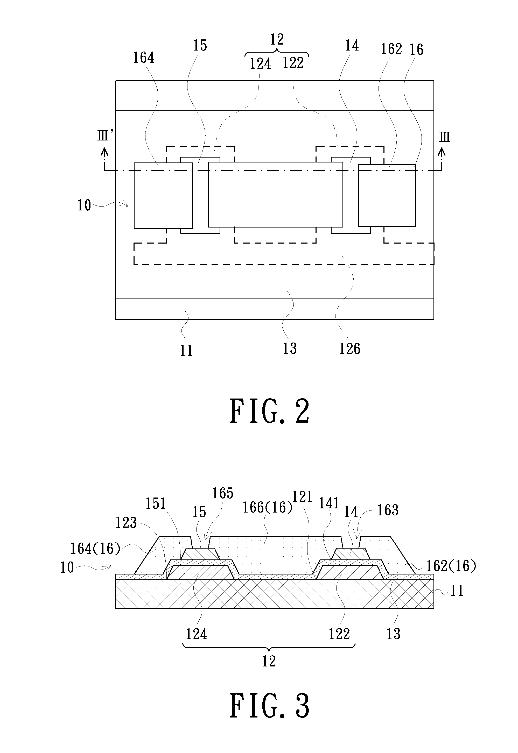
[0032]The TFT substrate 110 includes a substrate 11 and a TFT array 17 disposed on the substrate, wherein the substrate 11 may be a rigid substrate such as glass substrate and the TFT array 17 includes a plurality of TFT structures. FIG. 2 is a schematic top view illustrating a TFT structure of the present invention. FIG. 3 is a schematic cross-sectional view taken along a line III-III′ of the TFT structure shown in FIG. 2. Referring to FIGS. 2 and 3, each of the TFT structures 10 includes a gate layer 12, a gate insulator layer 13, a first semiconductor island 14 serving as a first channel island, a second semiconductor island 15 serving as a second channel island and a source and drain layer 16. It is to be noted that the term “source and drain layer” used herein indicates that a source electrode and a drain electrode are included in this layer to form a part of the TFT. The relative positions of the source electrode and the drain electrode are variable and the manufacturing proce...

second embodiment

[0036]Please refer to FIG. 4 and FIG. 5, in which a TFT structure of the present invention is schematically illustrated, and FIG. 5 is a schematic cross-sectional view taken along a line V-V′ of FIG. 4. In this embodiment, a TFT structure 20 includes a first semiconductor island 24 and a second semiconductor island 25, both of which have an “island out” structure. That is, opposite lateral sides 240 of the first semiconductor island 24 are outward offset from corresponding lateral sides 221 of the first gate electrode 222. The first semiconductor island 24 includes a central portion 243, a circumferential portion 242 and a bending portion 241 disposed between the central portion 243 and the circumferential portion 242, and having a turning corner. With the bending portion 241, the circumferential portion 242 deflects from the central portion 243 and extends downwards to surround the first gate electrode 222. For minimizing the area of the island, the bending portion 241 may be arran...

third embodiment

[0037]FIG. 6 is a schematic top view of a TFT structure in accordance with the present invention, and FIG. 7 is a schematic cross-sectional view taken along a line VII-VII′ of FIG. 6. Referring to FIGS. 6 and 7, a TFT structure 30 includes a first semiconductor island 34 having an “island in” structure and a second semiconductor island 35 having an “island out” structure, as described above.


PUM


Abstract

A thin film transistor (TFT) substrate includes a substrate which is a flexible substrate, and a TFT structure disposed on the substrate and including a gate layer, a gate insulator layer, a first channel island and a second channel island. The gate layer is disposed on the substrate and including a first gate electrode and a second gate electrode electrically connected to each other. The first and second gate electrodes are parts of the same TFT structure. The gate insulator layer covers the first and second gate electrodes. The first and second channel islands are disposed on the gate insulator layer and respectively correspond to the first and second gate electrodes. The source and drain layer is disposed on the gate insulator layer and next to the first and second channel islands, wherein the source and drain layer partially covers top surfaces of the first and second channel islands.

Description

CROSS-REFERENCE TO RELATED APPLICATIONS[0001]This application is a continuation-in-part application of an application Ser. No. 13 / 396,784, filed on Feb. 15, 2012, and based upon and claims the benefit of priority from the prior Taiwanese Patent Application No. 100109211, filed Mar. 17, 2011, the entire contents of which are incorporated herein by reference.FIELD OF THE INVENTION[0002]The present invention generally relates to a display device, and more particularly relates to a thin film transistor (TFT) substrate and a display device having the same.BACKGROUND OF THE INVENTION[0003]TFTs have been widely used in display applications such as liquid crystal displays (LCDs), electronic paper displays (EPDs), and organic light emitting diode displays (OLEDs).[0004]Generally, a TFT structure includes a substrate, a gate electrode, a gate insulator layer, a channel island, a source electrode, and a drain electrode. The gate electrode is disposed on the substrate, the gate insulator layer ...

Claims


Application Information

Patent Timeline
Patent Type & Authority Applications(United States)
IPC IPC(8): H01L27/12H01L51/05
CPCH01L27/1218H01L27/1222H01L27/1225H01L51/0545H01L29/41733H01L29/78696H01L29/78603H10K59/125H10K59/1213H10K10/484H10K10/466H10K77/111H10K2102/311H01L29/786
Inventor CHUANG, KAI-CHENGCHEN, CHAO-JUNGCHIANG, I-HSUAN
Owner E INK HLDG INC
Why Eureka
Try Eureka