Method and apparatus for driving an active matrix display panel

Inactive Publication Date: 2001-04-17
PANASONIC CORP
View PDF11 Cites 254 Cited by
  • Summary
  • Abstract
  • Description
  • Claims
  • Application Information

AI Technical Summary

Problems solved by technology

Conventional units such as the aforementioned, however, have poor light utilization efficiency, because the polarizing plate absorbs approximately 70% of incident light.
For this reason, the TN liquid crystal display panel has the prob

Method used


Image

  • Method and apparatus for driving an active matrix display panel
  • Method and apparatus for driving an active matrix display panel
  • Method and apparatus for driving an active matrix display panel

Examples


first embodiment

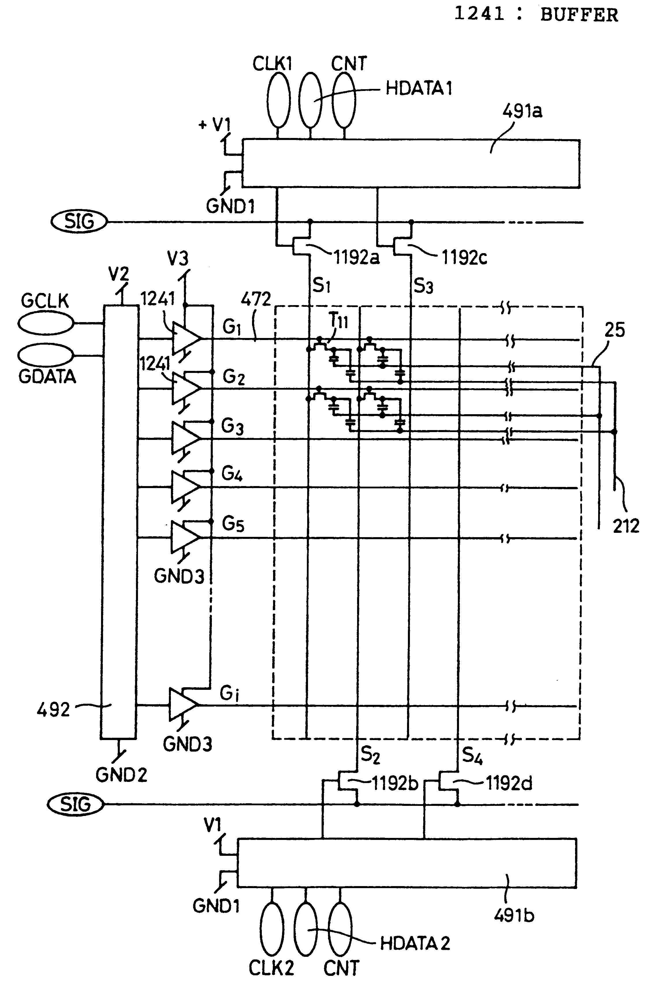
A description will hereinafter be made of an embodiment of a projection type display of the present invention in reference to the drawings. The constitution of a projection type display in the present invention is shown in FIG. 141. 1411 is a light source as light generation means, 1412 a color purity enhancement filter, and 1415 a projection lens as projection means.

The light source 1411 is constituted by a discharge lamp 1411a, a concave mirror 1411b, an ultraviolet-ray and infrared-ray (UVIR) cut filter 1411c. The discharge lamp 1411a is constituted by a metal halide lamp, and dysprosium (Dy) and neodymium (Nd) are enclosed within the light emitting tube. The emission spectrum is shown in FIG. 147. As evident in FIG. 147, in the spectral distribution of light emitted by the metal halide lamp, a great number of continuous emission spectra by dysprosium (Dy) and neodymium (Nd) and a bright line spectrum by mercury are present together. The concave mirror 1411b is formed with glass ...

second embodiment

Furthermore, as in the second embodiment, in the case where the difference in refractive index between a high refractive index layer and a low refractive index layer is small, if the absolute value of reflectance at a peak wavelength is attempted to be made high, there will be a need to increase the number of dielectric multilayer films, and depending on the number of films, there will be the fear that a crack will occur. In this case, the high refractive index layer can be constituted by a combination of TiO.sub.2 and ZnS whose refractive indexes are nearly the same and which has the property that the directions of internal stresses cancel out each other. The refractive indexes of the TiO.sub.2 and ZnS layers are nearly 2.30. In the TiO.sub.2 layer, tensile stress is produced, and in the ZnS layer, compression stress is produced. Therefore, for example, if the layers in the high refractive index multilayer film are respectively constituted by three layers consisting of TiO.sub.2, Z...


PUM

PropertyMeasurementUnit
Thicknessaaaaaaaaaa
Thicknessaaaaaaaaaa
Thicknessaaaaaaaaaa

Abstract

An array substrate 12 is formed with pixel electrodes 14 in the form of a matrix. The pixel electrode 14 is connected to a thin film transistor 155. The thin film transistor 155 is formed with a light shielding film 152 consisting of resin for preventing an entry of light into the thin film transistor 155. A polymer dispersion liquid crystal layer 21 is interposed between a counter electrode 25 and the pixel electrode 14. A substrate 11 is formed with a color filter 151 having red (R), green (G), and blue (B). The color filter 151 is formed from dielectric multilayer film or organic material. The counter electrode 25 is formed above the color filter 155, and the counter electrode 25 and the liquid crystal layer 21 are bonded together by an adhesive layer 371.

Description

1. Field of the InventionThe present invention relates to a display panel, a method of fabricating the display panel, a method of driving the display panel, a method of correcting a defect in the display panel, and a display employing the display panel.2. Description of the Related ArtTwisted nematic (TN) liquid crystals making use of the optical rotation of a liquid crystal have presently been employed in available projection displays (liquid crystal projectors) and view finders.The TN liquid crystal display panel employing the TN liquid crystal needs to employ a polarizing plate to modulate light.Conventional units such as the aforementioned, however, have poor light utilization efficiency, because the polarizing plate absorbs approximately 70% of incident light. For this reason, the TN liquid crystal display panel has the problem that high brightness display cannot be realized.The TN liquid crystal display panel also needs a rubbing process, because there is a need to orient liqu...

Claims


Application Information

Patent Timeline
IPC IPC(8): G09G3/36H04N9/31G02F1/13G02F1/1368G02F1/1333G02F1/1334G02F1/1335G02F1/1343G02F1/1347G02F1/1362
CPCG02F1/1334G02F1/133526G09G3/3648H04N9/3105H04N9/3144H04N9/3167H04N9/3197G02F1/133345G02F1/133553G02F1/134363G02F1/13454G02F1/1347G02F1/136259G02F1/1368G02F2001/133521G02F2201/34G02F2202/104G09G3/3614G09G3/3655G09G2300/0434G09G2310/0283G02F1/133521
Inventor TAKAHARA, HIROSHI
Owner PANASONIC CORP
Why Eureka
Try Eureka