2D/3D switchable parallax barrier display
a parallax barrier and display technology, applied in optics, instruments, electrical equipment, etc., can solve the problems of the conductivity of transparent materials of lc driving (i.e. ito), complicating this countermeasure, etc., to reduce the noise of the sensing electrode, reduce the noise of the driving scheme, and suppress the voltage fluctuation
- Summary
- Abstract
- Description
- Claims
- Application Information
AI Technical Summary
Benefits of technology
Problems solved by technology
Method used
Image

Examples
first embodiment
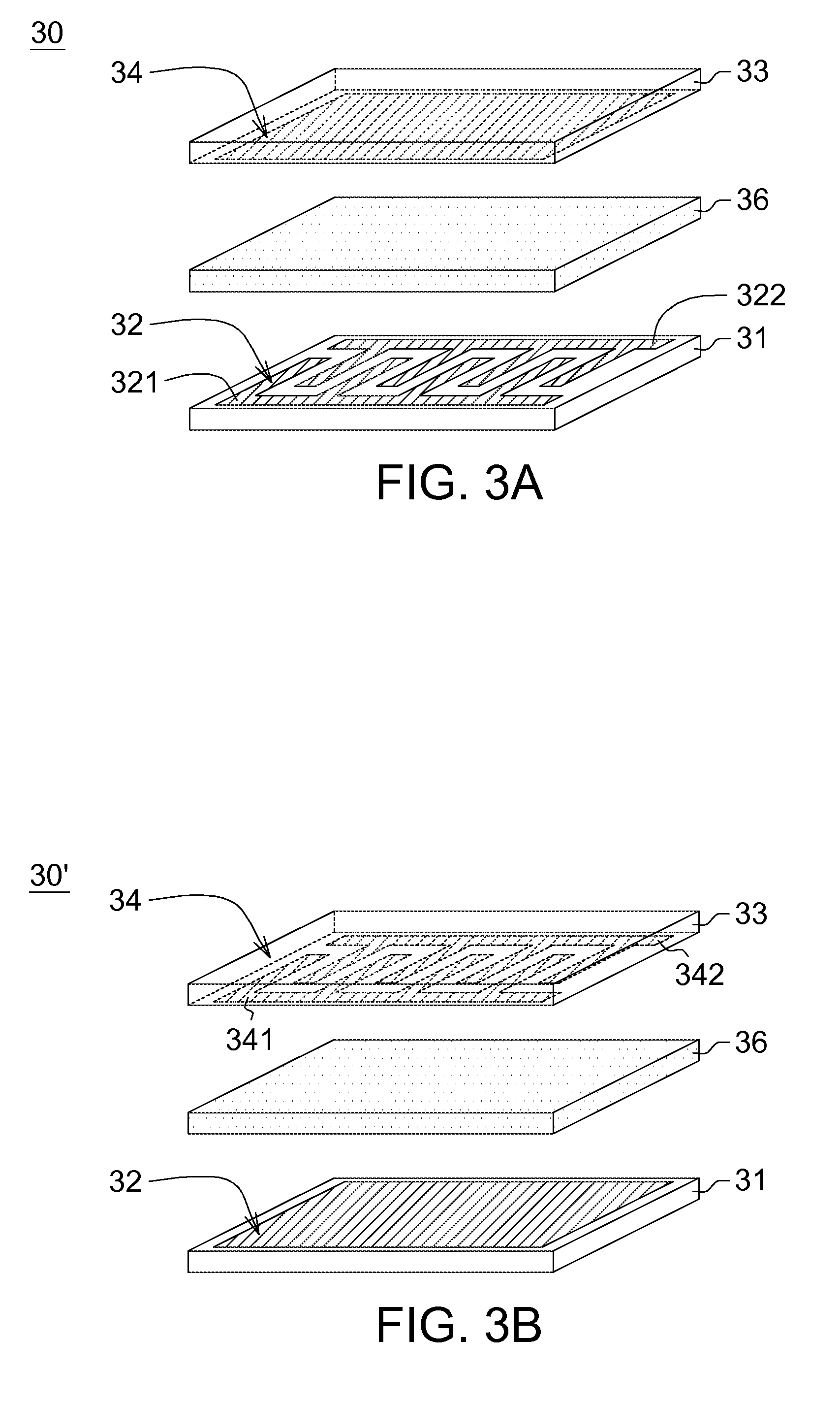
[0036]FIG. 3A shows a parallax barrier of a 2D / 3D switchable display according to the first embodiment of the present disclosure. FIG. 3B shows another parallax barrier of a 2D / 3D switchable display according to the first embodiment of the present disclosure. The difference between the parallax barriers 30 and 30′ of FIG. 3A and FIG. 3B is a switch of electrode arrangement.
[0037]Please refer to FIG. 3A. The parallax barrier 30 could be disposed on a display module (not shown in FIG. 3A) and is a LCD panel comprising a bottom substrate 31 having a bottom electrode layer 32, a top substrate 33 having a top electrode layer 34, and a LC layer 36 sandwiched between the bottom substrate 31 and the top substrate33. The bottom electrode layer 32 and the top electrode layer 34 are coupled to different voltage sources.
[0038]In FIG. 3A, the upper electrode layer 34 is a flat plane, and the bottom electrode layer 32 at least comprises two finger electrodes interlaced to each other and separated...
second embodiment
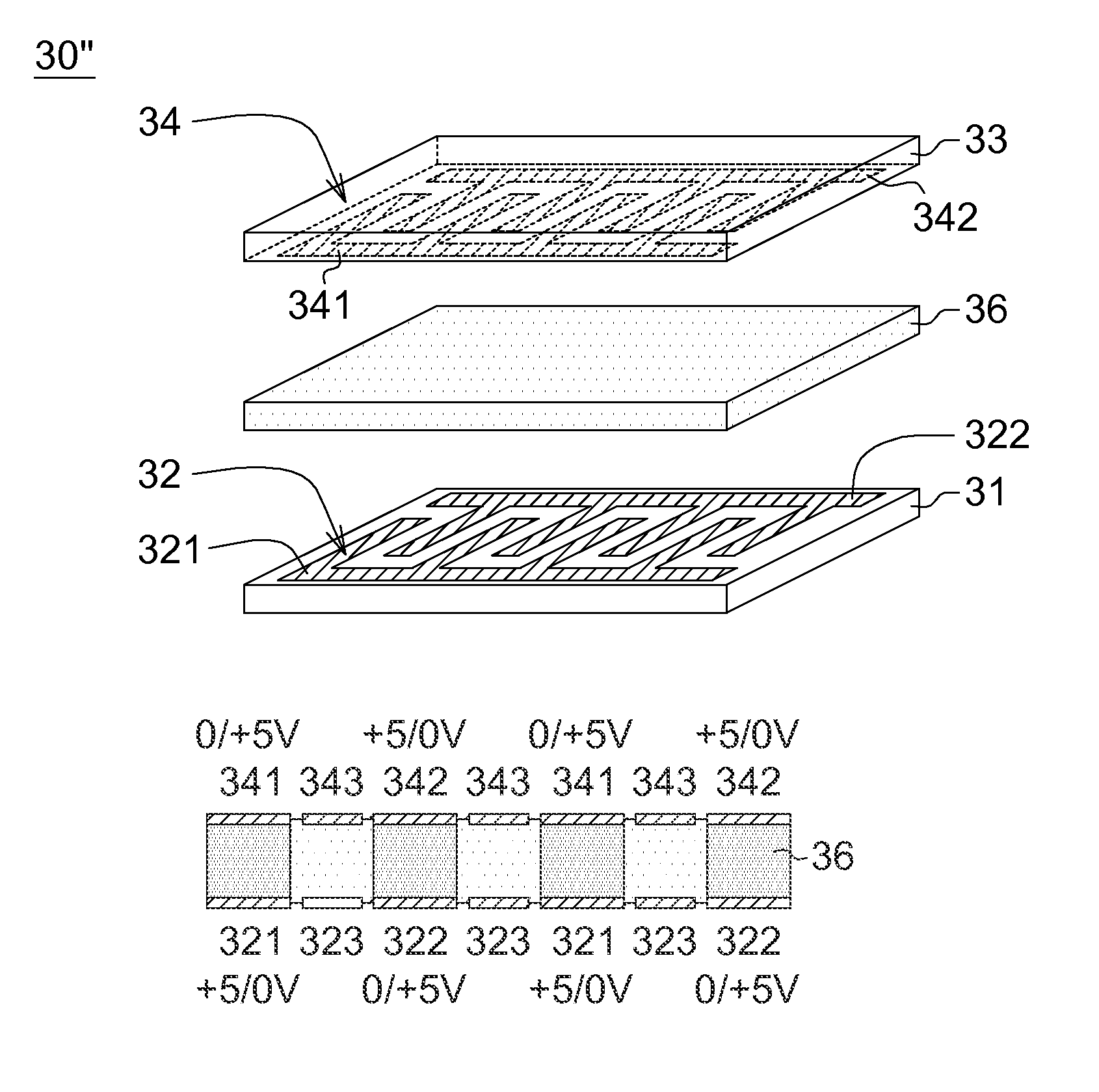
[0044]FIG. 7 shows a parallax barrier of a 2D / 3D switchable display according to the second embodiment of the present disclosure. Components of the parallax barrier 30″ of FIG. 7 common to that of the parallax barrier 30 of FIG. 3A retain the same reference numbers. Structural difference between the parallax barriers of the second and the first embodiment are the configurations of the top electrode layer.
[0045]Similarly, the parallax barrier 30″ includes a bottom substrate 31 having a bottom electrode layer 32, a top substrate 33 having a top electrode layer 34, and a LC layer 36 sandwiched between the bottom substrate 31 and the top substrate 33. One or more of the voltage sources are, not limited, coupled to the bottom electrode layer 32 and the top electrode layer 34. Practically, the electrodes driven by the same or similar signal in operation, e.g., applied with the same or similar voltage could be coupled to the same voltage source.
[0046]In the second embodiment, each of the u...
third embodiment
[0055]FIG. 12 illustrates a top electrode layer and a bottom electrode layer of a parallax barrier of a 2D / 3D switchable display according to the third embodiment of the present disclosure. In FIG. 12, the bottom substrate, the top substrate, and a LC layer sandwiched between the bottom substrate and the top substrate of the parallax barrier are not shown in the drawing to avoid obscuring the third embodiment. Also, components of FIG. 12 common to that of the parallax barrier 30″ of FIG. 7 retain the same reference numbers. Structural difference between the parallax barriers of the second and the third embodiment are the configurations of the top electrode layer.
[0056]Similarly, a bottom electrode 32 comprises a first finger electrode 321, a second finger electrode 322 interlaced with the first finger electrode 321 and separated with a space, and a bottom middle electrode 323 optionally disposed between the first finger electrode 321 and the second finger electrode 322. A top electr...
PUM
| Property | Measurement | Unit |
|---|---|---|
| voltages | aaaaa | aaaaa |
| voltages | aaaaa | aaaaa |
| voltages | aaaaa | aaaaa |
Abstract
Description
Claims
Application Information
 - R&D Engineer
- R&D Manager
- IP Professional
- Industry Leading Data Capabilities
- Powerful AI technology
- Patent DNA Extraction
Browse by: Latest US Patents, China's latest patents, Technical Efficacy Thesaurus, Application Domain, Technology Topic.
© 2024 PatSnap. All rights reserved.Legal|Privacy policy|Modern Slavery Act Transparency Statement|Sitemap