Formation of liner and barrier for tungsten as gate electrode and as contact plug to reduce resistance and enhance device performance

a gate electrode and tungsten technology, applied in the direction of coatings, transistors, basic electric elements, etc., can solve the problems of reducing size, incompatible with many device integration processes, and various issues with depositing and using tin films

Active Publication Date: 2015-09-08
APPLIED MATERIALS INC
View PDF20 Cites 6 Cited by
  • Summary
  • Abstract
  • Description
  • Claims
  • Application Information

AI Technical Summary

Problems solved by technology

While titanium tetrachloride (TiCl4)-based TiN processes provide improved step coverage, the deposition is usually performed at temperatures much greater than 400° C., which is incompatible with many device integration processes.
Meanwhile, various issues arise with depositing and using TiN films, especially as feature sizes decrease.
One problem with TiN is that TiN has poor diffusion resistance, so that halide elements such as Cl (in CVD-TiN with TiCl4) and F (in CVD-W bulk with WF6) may diffuse into the device during subsequent thermal processing, thereby adversely increasing resistivity of the film and cause interface issues.

Method used


Image

  • Formation of liner and barrier for tungsten as gate electrode and as contact plug to reduce resistance and enhance device performance
  • Formation of liner and barrier for tungsten as gate electrode and as contact plug to reduce resistance and enhance device performance
  • Formation of liner and barrier for tungsten as gate electrode and as contact plug to reduce resistance and enhance device performance

Examples


Embodiment Construction

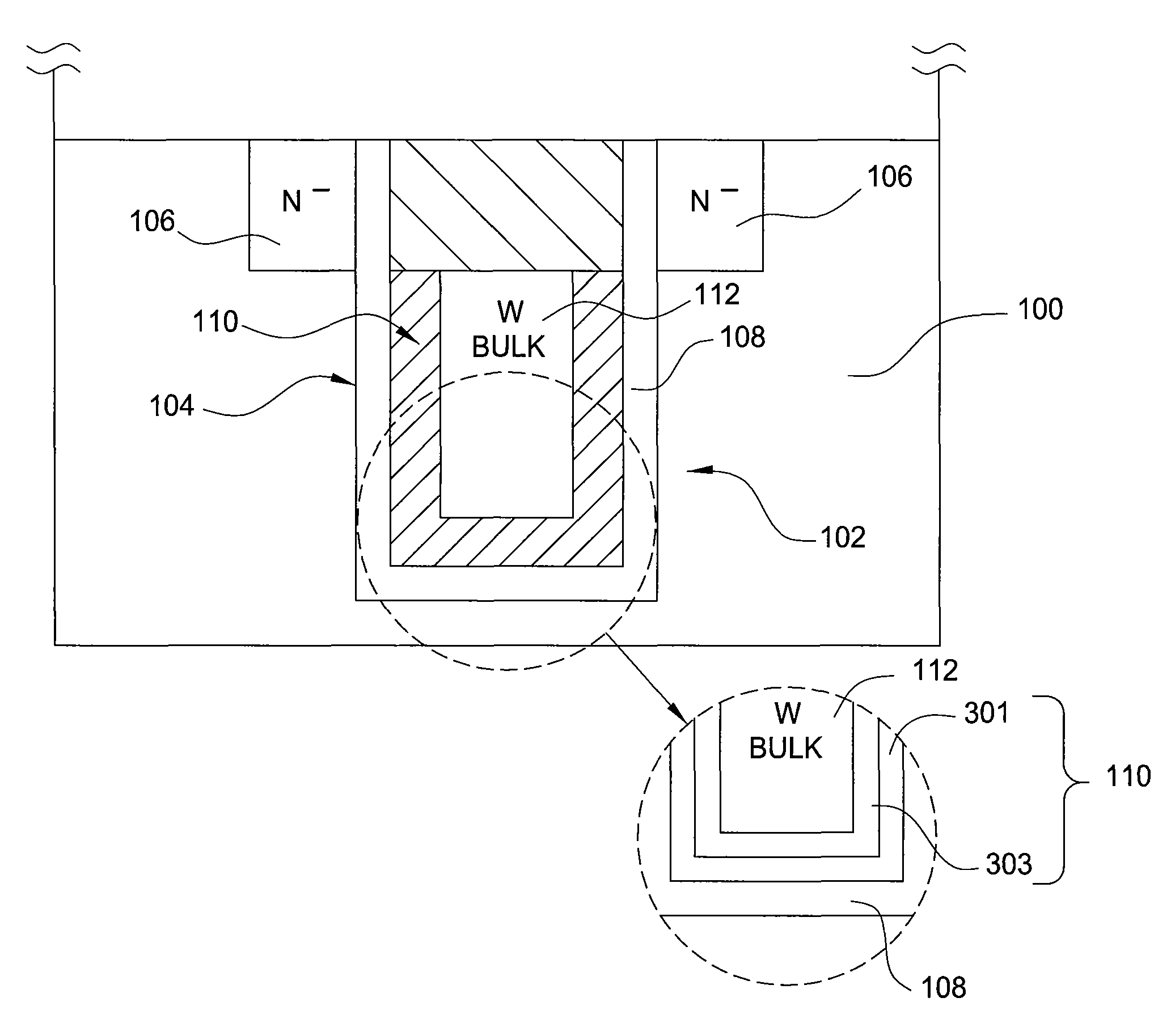
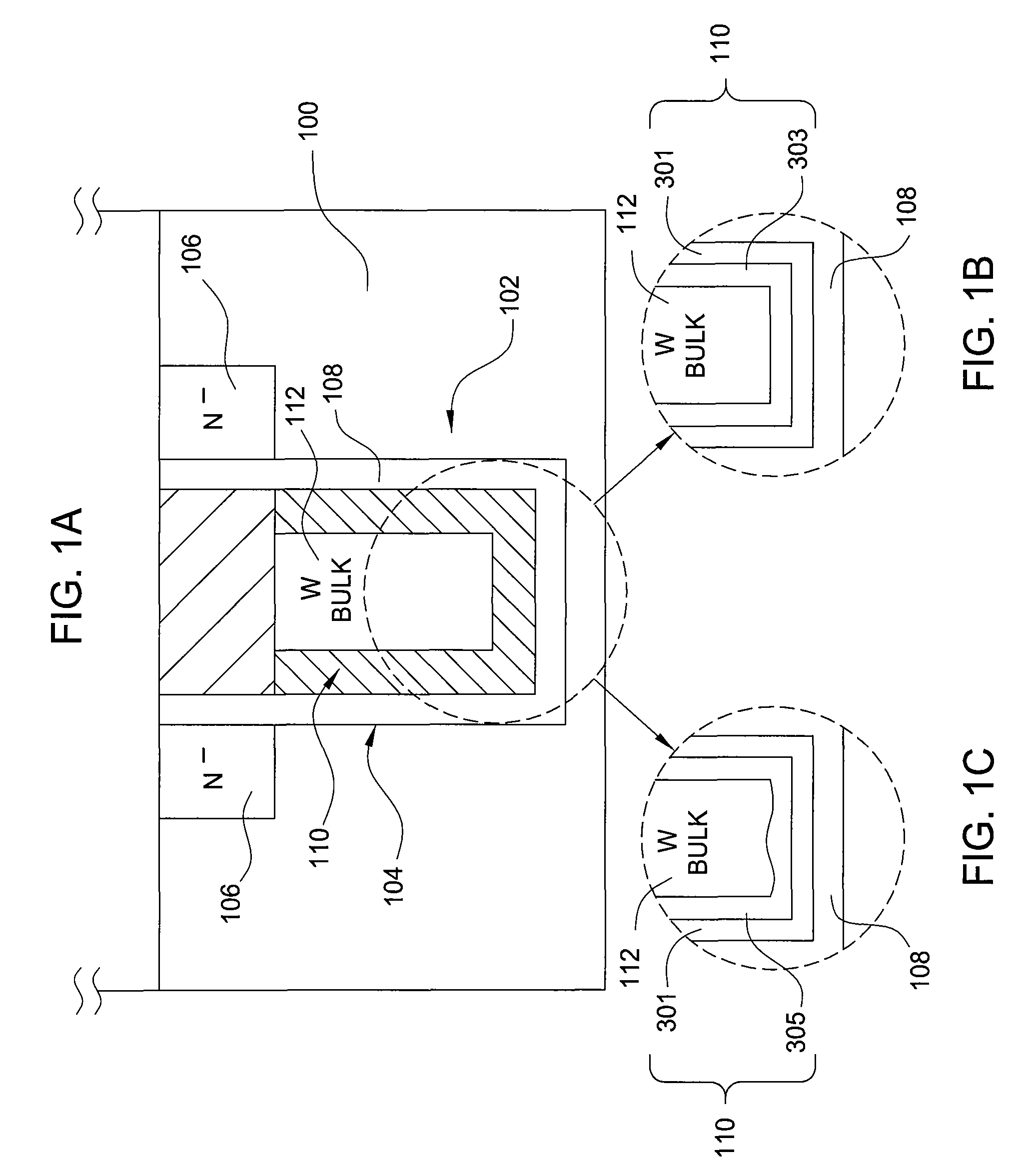
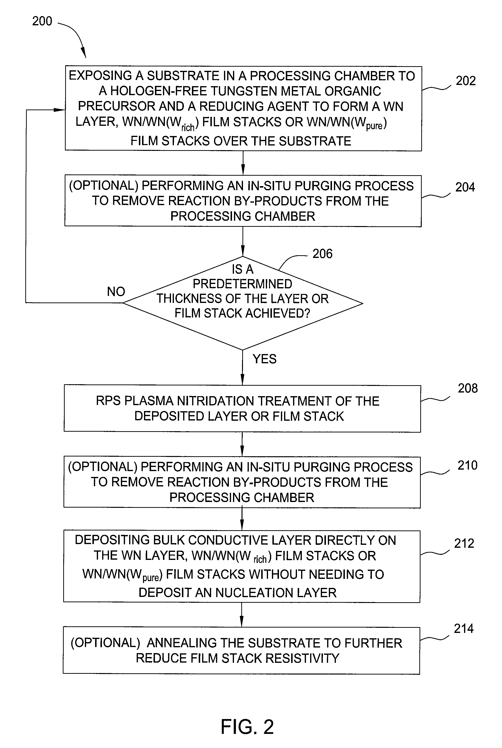
[0016]Embodiments of the present invention provide a method and an integrated film stacks for contact plugs, buried word lines used in DRAM, or other logic device applications requiring a contact barrier or metal electrodes having feature size less than 40 nm. In various embodiments of the present invention, a halogen-free MOCVD or MOALD process is used to deposit an integrated WN, WN / WN(Wrich), or WN / WN(Wpure) film stacks, which may serve as a strong barrier to prevent the underlying region from fluorine penetration during subsequent gate metallization process. The integrated film stacks of the present invention can achieve void free (>90% WN step coverage) gap fill of high aspect ratio features and advantageously eliminates the need to deposit a high resistive nucleation layer prior to deposition of the W gate metallization since the thin tungsten rich tungsten nitride WN(Wrich) layer or tungsten pure tungsten nitride WN(Wpure) layer formed at the surface of the WN layer serve as ...


PUM

PropertyMeasurementUnit
temperaturesaaaaaaaaaa
feature sizeaaaaaaaaaa
aspect ratioaaaaaaaaaa

Abstract

The invention provides a method of forming a film stack on a substrate, comprising depositing a tungsten nitride layer on the substrate, subjecting the substrate to a nitridation treatment using active nitrogen species from a remote plasma, and depositing a conductive bulk layer directly on the tungsten nitride layer without depositing a tungsten nucleation layer on the tungsten nitride layer as a growth site for tungsten.

Description

BACKGROUND OF THE INVENTION[0001]1. Field of the Invention[0002]Embodiments of the present invention generally relate to a method and improved film stacks for contact plug or gate electrode used in DRAM applications.[0003]2. Description of the Related Art[0004]Tungsten-containing films are typically used in multiple applications for semiconductor device fabrication. For example, metallic tungsten (W) has been a primary conductor for contacts and vias. Metallic tungsten is also used in bit lines. The typical film stack in use currently is Ti / TiN nucleation / CVD-W bulk, with the titanium (Ti) / titanium nitride (TiN) layers acting as liner or barrier films.[0005]While titanium tetrachloride (TiCl4)-based TiN processes provide improved step coverage, the deposition is usually performed at temperatures much greater than 400° C., which is incompatible with many device integration processes. Meanwhile, various issues arise with depositing and using TiN films, especially as feature sizes decr...

Claims


Application Information

Patent Timeline
Patent Type & Authority Patents(United States)
IPC IPC(8): H01L23/532C23C16/34H01L23/485H01L21/285H01L21/321H01L27/108H01L21/28H01L21/768H01L29/423
CPCH01L23/485C23C16/34H01L21/28088H01L21/28556H01L21/321H01L21/76846H01L21/76856H01L21/76877H01L21/76883H01L21/76886H01L23/53266H01L27/10891H01L2924/0002H01L2924/00H01L29/4236H10B12/488
Inventor LEE, SANG-HYEOBYU, SANG HOLEE, WEI TIGANGULI, SESHADRIHA, HYOUNG-CHANKIM, HOON
Owner APPLIED MATERIALS INC
Why Eureka
Try Eureka