Selective etching of silicon nitride

a silicon nitride and selective etching technology, applied in the direction of basic electric elements, semiconductor/solid-state device manufacturing, electric apparatus, etc., can solve the problem that the aforementioned high selectivity process cannot be used to clean silicon nitride from the surface without damaging the oxide layer, and increase the chances of electrical interference. the effect of selective oxidation

Inactive Publication Date: 2009-04-23
APPLIED MATERIALS INC
View PDF9 Cites 284 Cited by
  • Summary
  • Abstract
  • Description
  • Claims
  • Application Information

AI Technical Summary

Benefits of technology

The present invention provides a way to remove a layer made up of both silicon and nitrogen on a semiconductor device by using a combination of gases containing H2, NF3, and optionally NH3. This technique allows for controlled removal without damaging other layers or structures on the chip.

Problems solved by technology

The technical problem addressed in this patent text relates to improving etch processes for effectively removing silicon nitride materials while maintaining good quality of underlying oxide layers without causing damage or defects in the process.

Method used


Image

  • Selective etching of silicon nitride
  • Selective etching of silicon nitride
  • Selective etching of silicon nitride

Examples


Embodiment Construction

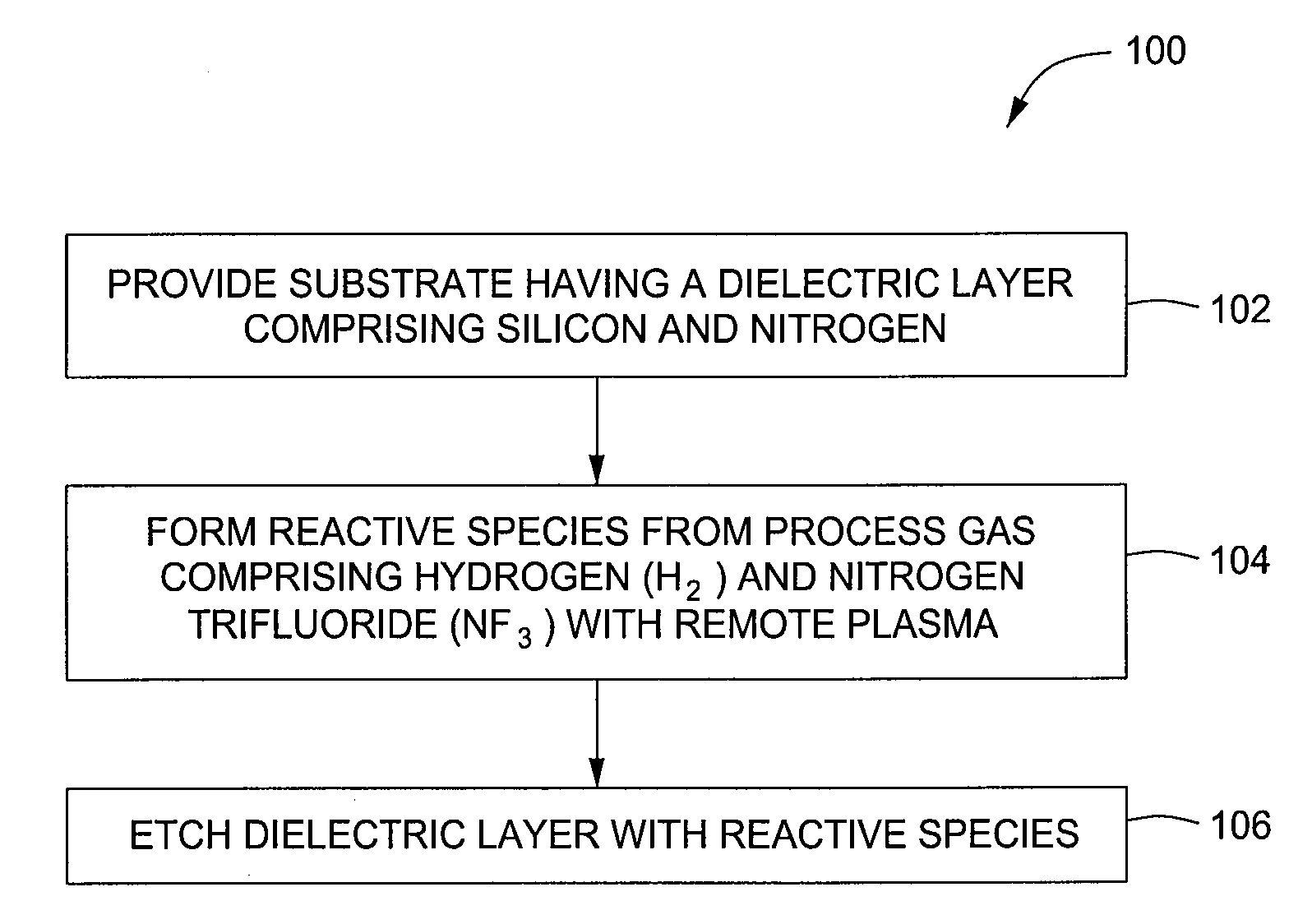
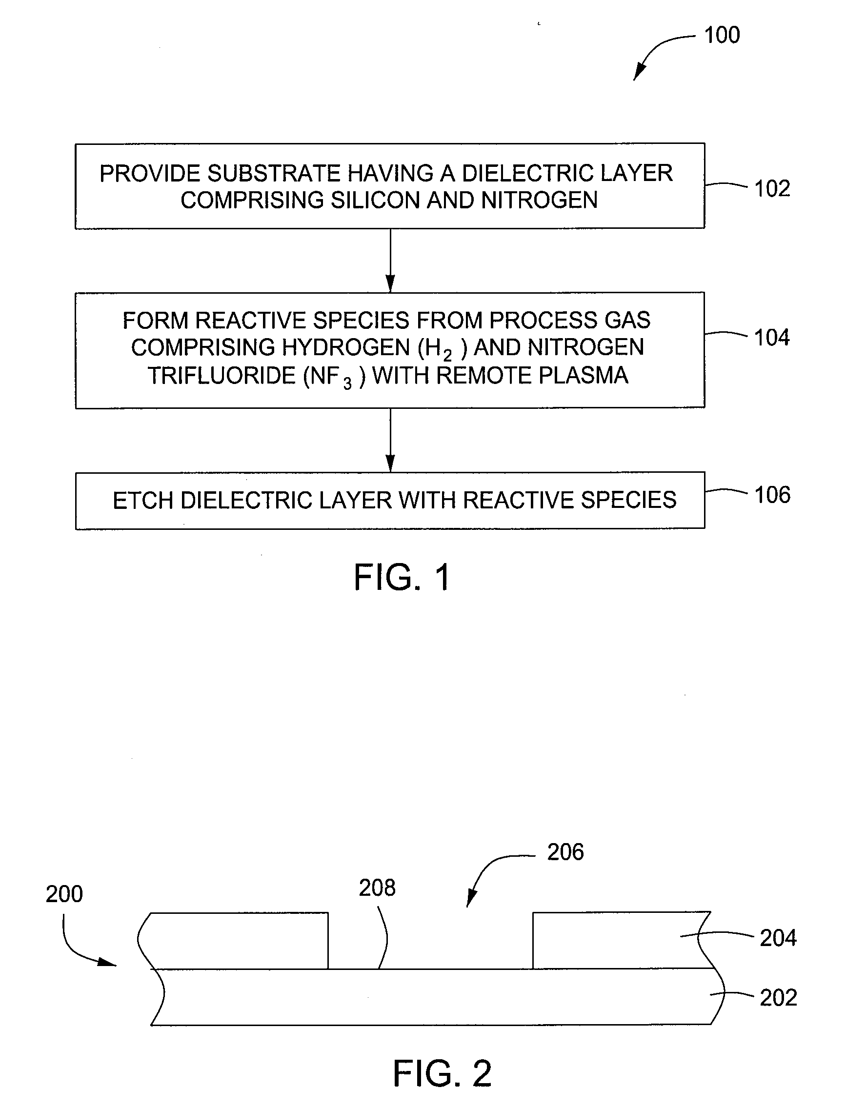
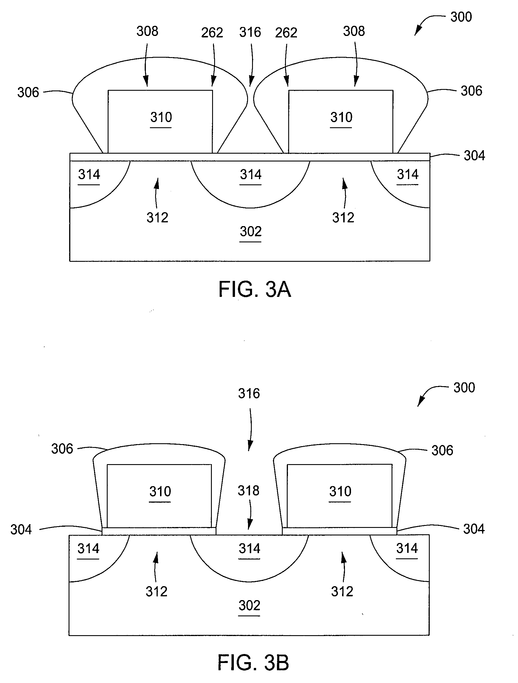
[0021]Embodiments of the present invention provide methods for etching dielectric layers comprising silicon and nitrogen on a substrate. Embodiments of the present invention may advantageously provide selective etching of the dielectric layer. In some embodiments, a process gas comprising hydrogen (H2), nitrogen trifluoride (NF3), and, optionally, ammonia (NH3) may be used to form a plasma. By adjusting the flow rate ratio of the constituents of the process gas, the etch selectivity of the dielectric layer to an oxide layer may be controlled between about 0.8 to about 4, thereby facilitating processing flexibility in etching the dielectric layer. In some embodiments, the selective etching methods may selectively remove at least portions of the dielectric layer, either isotropically or anisotropically. In some embodiments, the etch selectivity of the dielectric layer to at least one of a metal, a metal silicide, or an oxide layer may be greater than 1, and / or up to about 4. Hence, th...


PUM


Abstract

Methods for etching dielectric layers comprising silicon and nitrogen are provided herein. In some embodiments, such methods may include providing a substrate having a dielectric layer comprising silicon and nitrogen disposed thereon, forming reactive species from a process gas comprising hydrogen (H2) and nitrogen trifluoride (NF3) using a remote plasma; and etching the dielectric layer using the reactive species. In some embodiments, an oxide layer is disposed adjacent to the dielectric layer. In some embodiments, the flow rate ratio of the process gas can be adjusted such that an etch selectivity of the dielectric layer to at least one of the oxide layer or the substrate is between about 0.8 to about 4.

Description


Claims


Application Information

Patent Timeline
Owner APPLIED MATERIALS INC
Why Eureka
Try Eureka