Rps assisted RF plasma source for semiconductor processing

a technology of assisted rf plasma and semiconductor processing, which is applied in the direction of vacuum evaporation coating, semiconductor/solid-state device testing/measurement, coating, etc., can solve the problem of unwanted particle contamination on the substrate surface, ion bombardment of the powered electrode, and a portion of the protective coating layer may fall o

Active Publication Date: 2015-08-06
APPLIED MATERIALS INC
View PDF3 Cites 320 Cited by
  • Summary
  • Abstract
  • Description
  • Claims
  • Application Information

AI Technical Summary

Benefits of technology

The patent describes a substrate processing system with two processing chambers. The first chamber has a primary plasma source and an ion suppression element, while the second chamber has a primary plasma source and an ion suppression element. Both chambers have a gas distribution plate and substrate support for processing substrates. The system allows for independent control of plasma excitation and substrate processing in each chamber, resulting in improved processing efficiency and flexibility.

Problems solved by technology

The patent text discusses the problem of plasma processing chambers causing particle contamination on substrate surfaces due to ion bombardment of the electrodes. The text aims to provide an apparatus and process that can effectively reduce the generation of contaminating particles and maintain high process yield.

Method used


Image

  • Rps assisted RF plasma source for semiconductor processing
  • Rps assisted RF plasma source for semiconductor processing
  • Rps assisted RF plasma source for semiconductor processing

Examples


Embodiment Construction

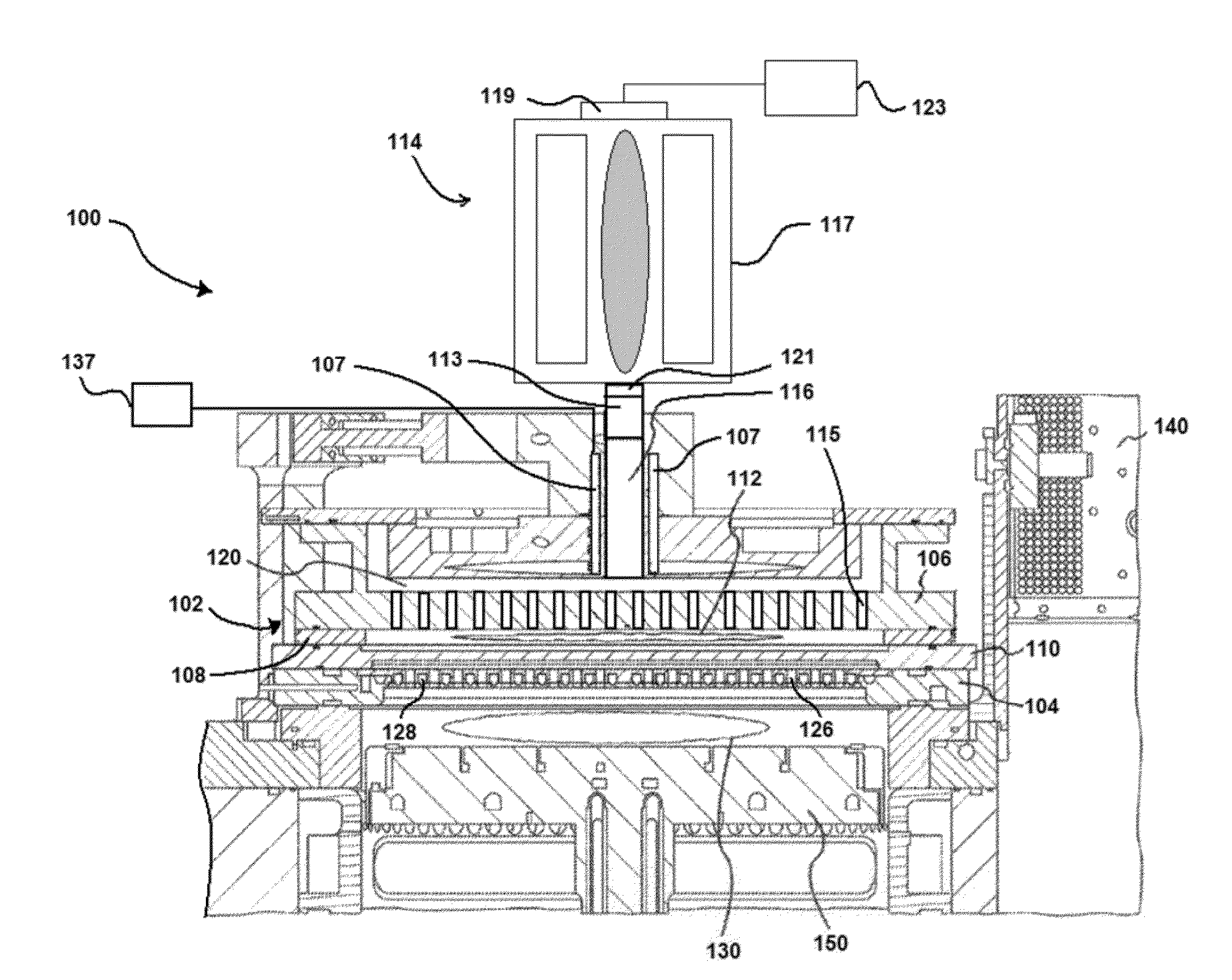
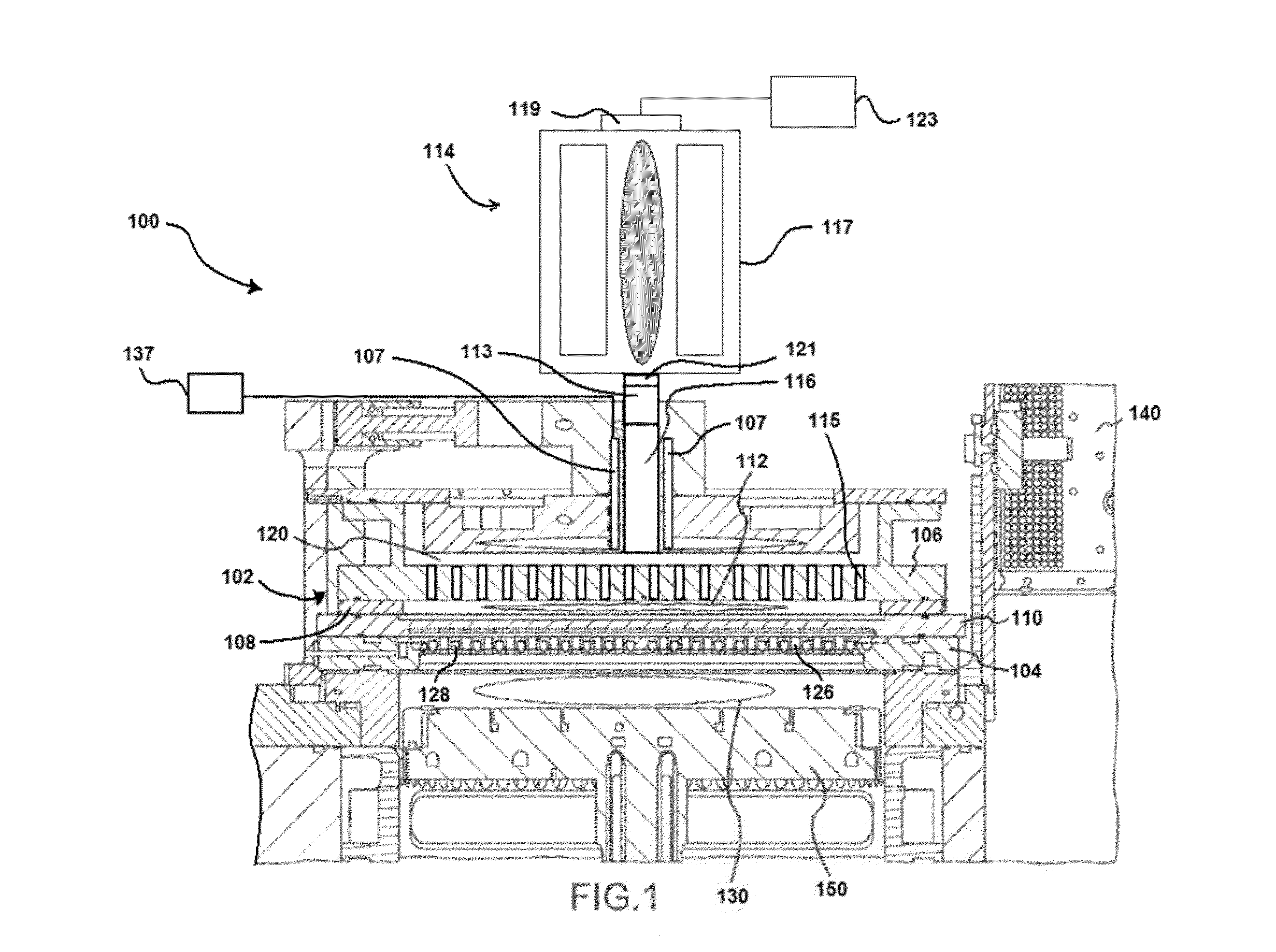
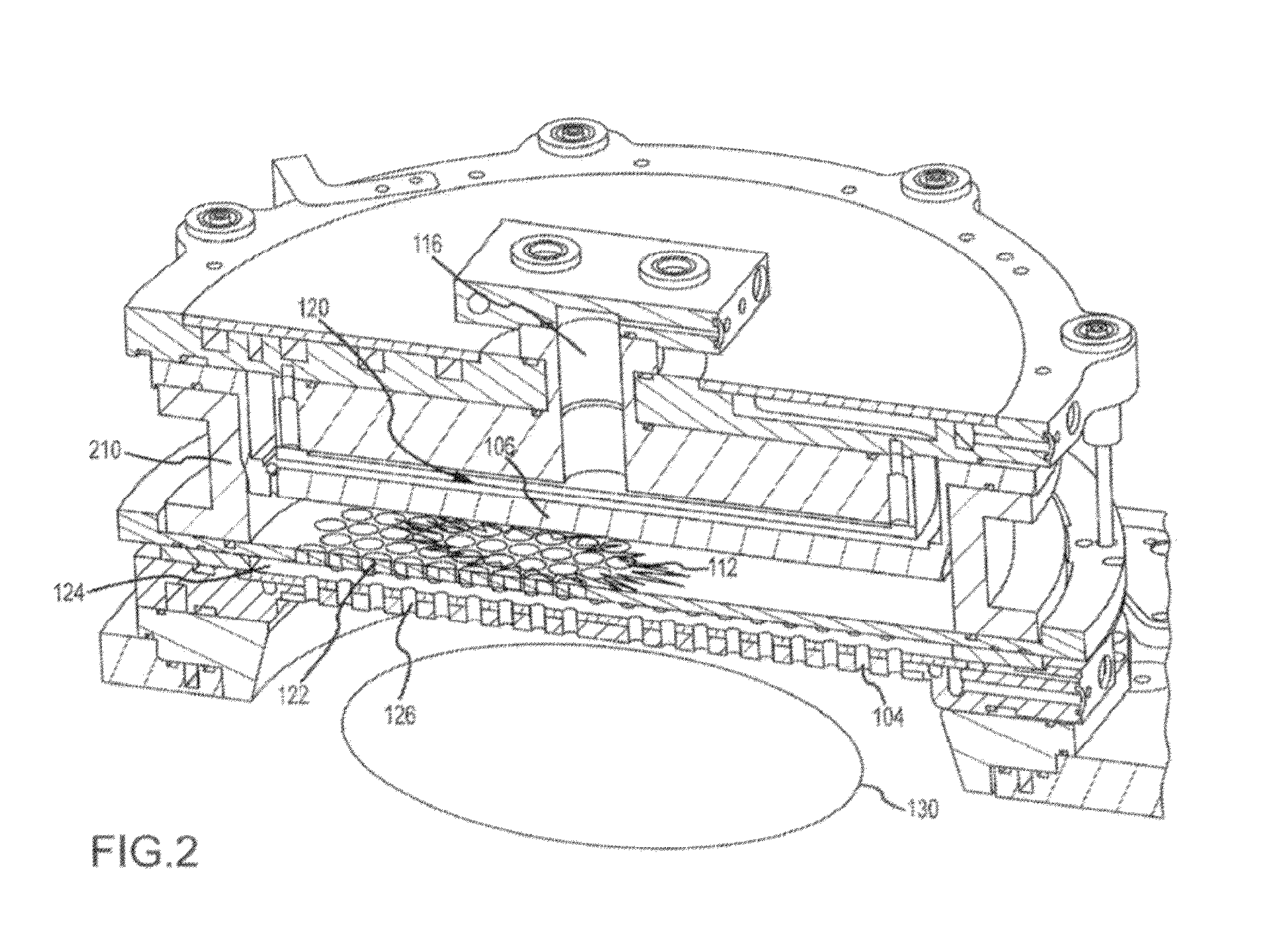
[0017]Embodiments of the disclosure relate to a hybrid plasma processing system combining a primary plasma source, such as capacitively coupled plasma (CCP) source or inductively coupled plasma (ICP) source, and a secondary plasma source, such as remote plasma source (RPS). The primary plasma source may be positioned adjacent to a substrate processing region and the secondary plasma source may be positioned further away from the substrate processing region. In one embodiment, the primary plasma source is positioned between the substrate processing region and the secondary plasma source. Depending upon process requirements, the primary plasma source and the secondary plasma source may subsequently turn on in any desired order for substrate processing. Alternatively, either the primary plasma source or the secondary plasma source is turned on for substrate processing. In cases where RPS and CCP are used for plasma generation and substrate processing, the RPS shares or relieves the pow...


PUM

PropertyMeasurementUnit
Thicknessaaaaaaaaaa
Pressureaaaaaaaaaa

Abstract

Embodiments of the disclosure generally relate to a hybrid plasma processing system incorporating a remote plasma source (RPS) unit with a capacitively coupled plasma (CCP) unit for substrate processing. In one embodiment, the hybrid plasma processing system includes a CCP unit, comprising a lid having one or more through holes, and an ion suppression element, wherein the lid and the ion suppression element define a plasma excitation region, a RPS unit coupled to the CCP unit, and a gas distribution plate disposed between the ion suppression element and a substrate support, wherein the gas distribution plate and the substrate support defines a substrate processing region. In cases where process requires higher power, both CCP and RPS units may be used to generate plasma excited species so that some power burden is shifted from the CCP unit to the RPS unit, which allows the CCP unit to operate at lower power.

Description


Claims


Application Information

Patent Timeline
Owner APPLIED MATERIALS INC
Why Eureka
Try Eureka