Plasma immersion ion implantation process

a technology of ion implantation and plasma, which is applied in the direction of plasma technique, vacuum evaporation coating, coating, etc., can solve the problems of high sheet resistance, low quality deposited layer that is less crystalline and more amorphous, and rough surface of the wafer surfa

Inactive Publication Date: 2006-04-20
APPLIED MATERIALS INC
View PDF99 Cites 333 Cited by
  • Summary
  • Abstract
  • Description
  • Claims
  • Application Information

AI Technical Summary

Benefits of technology

[0009] The wafer support can be a high contact force electrostatic chuck having a flat polished workpiece contact surface, in which case a workpiece temperature controller governs a wafer clamping voltage of the electrostatic chuck. The bias source can be one of (a) an RF source, (b) a D.C. source. The plasma source power applicator can include a toroidal core of a magnetic material surrounding a section of the reentrant conduit and a conductor wound around the core and coupled to the RF source power generator.

Problems solved by technology

Such a cleaning process can be carried out very rapidly using a plasma process, but this can leave the wafer surface very rough, leading to inferior results.
For example, a rough surface that is ion implanted with a dopant material can have an excessive sheet resistance.
Deposition of an epitaxial layer (by a plasma enhanced chemical vapor deposition process, for example) on a rough surface can result in a low quality deposited layer that is less crystalline and more amorphous.
This approach leaves the smoothest wafer surface but can be unacceptably slow, and in many cases should be carried out at a sufficiently high temperature to activate the gas species.
Such a high temperature can exceed the wafer process thermal budget.
The problem is that the external feed from the RPS chamber to the main chamber holding the wafer does not provide a uniform distribution of the neutrals or radicals over the wafer surface, so that the wafer cannot be cleaned uniformly.
Typically, the radicals or neutrals from the RPS chamber are fed to a side port of the main chamber, leading to the non-uniformity.
Unfortunately, plasma cleaning process are so fast that they tend to consume a relatively large fraction of the chamber surfaces and elements (such as process kits), and therefore are extremely costly insofar as they require frequent replacement of chamber interior parts and materials.
The minimum consumption of chamber interior elements for a thorough cleaning is obtained using cleaning gases without a plasma, but this approach is too time-consuming.
The problem with this approach is that distribution within the main chamber of the dissociated cleaning gases from an external remote plasma source (RPS) chamber is non-uniform, so that the main chamber cannot be cleaned uniformly.
This is because the external feed from the RPS chamber to the main chamber does not provide a uniform distribution of the neutrals or radicals within the main chamber.
One problem encountered in plasma immersion ion implantation is that the dopant-containing process gas can sometimes form a film on the surface being implanted that can block the implantation or distort the implant depth profile from the desired one.
Such an unwanted film can, in some cases, distort the ion implantation depth profile (or render it difficult to control during implantation), so that the resulting depth profile may not be ideal.
Another problem is that the ion bombardment can etch away the surface being implanted, removing much of the implanted ions and thereby attenuating the desired effects of the implantation process.
In a dopant implantation process in a semiconductor layer, this problem manifests itself as a high sheet resistance.
Another problem that can arise in any plasma process is contamination on the wafer backside that degrades subsequent wafer processing steps.
Metallic contamination occurs because in many cases the insulating layer on the ESC surface is a metal-containing compound such as AlN.
AlN particles scraped onto the wafer backside from the ESC can be dissociated in later plasma process steps to free the Al species and form metallic contamination, which can degrade process performance.

Method used


Image

  • Plasma immersion ion implantation process
  • Plasma immersion ion implantation process
  • Plasma immersion ion implantation process

Examples


working examples

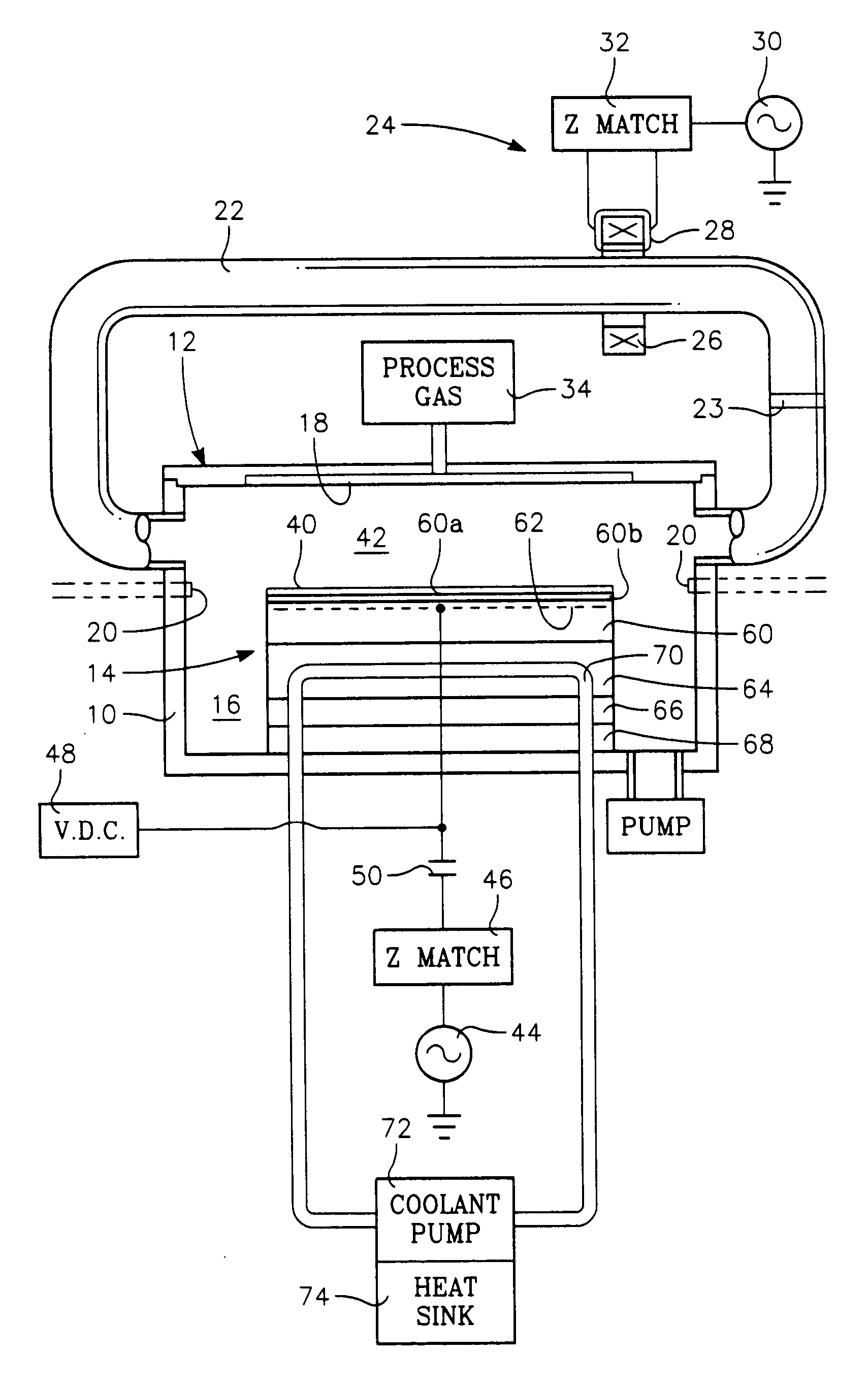
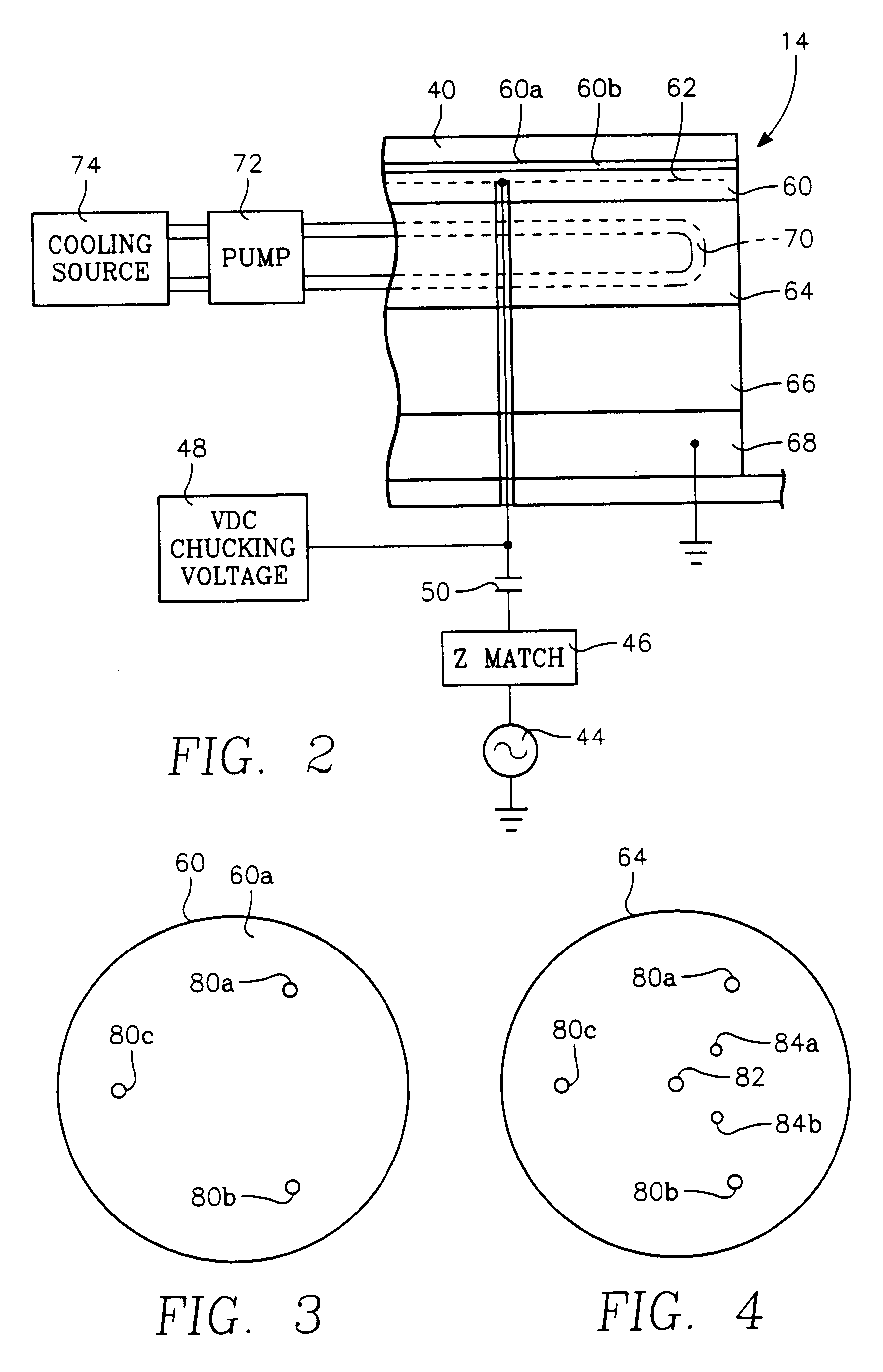
[0092] Plasma immersion ion implantation using a fluoride dopant gas (such as BF3) with a bias voltage of 1 kV can be carried out using ESC temperature in a range between −40 and +60 degrees C., the preferred range being between 0 and +40 degrees C., a chamber wall temperature in the range of 0 to 120 degrees C., the preferred range being 20 to 80 degrees C. If the bias voltage is increased to 8 kV, then the maximum ESC temperature decreases to 60 degrees C. and the preferred maximum ESC temperature decreases to 20 degrees C. The foregoing assumes that Si etching loss be limited to much less than 10 Angstroms. For a hydride dopant gas, the temperature range tends to be higher, because, compared to fluoride dopant gases, hydride dopant gases tend to etch less and promote more deposition: at 1 kV bias and 500 watt source power, the ESC temperature range is 0 to 80 degrees C., the preferred range being 20 to 60 degrees C. At 8 kV, a lower temperature is better, the range being decrease...


PUM

PropertyMeasurementUnit
dielectric constantaaaaaaaaaa
pressureaaaaaaaaaa
temperatureaaaaaaaaaa

Abstract

A method of processing a workpiece includes placing the workpiece on a workpiece support pedestal in a main chamber with a gas distribution showerhead, introducing a process gas into a remote plasma source chamber and generating a plasma in the remote plasma source chamber, transporting plasma-generated species from the remote plasma source chamber to the gas distribution showerhead so as to distribute the plasma-generated species into the main chamber through the gas distribution showerhead, and applying plasma RF power into the main chamber.

Description

CROSS-REFERENCE TO RELATED APPLICATIONS [0001] This application is a continuation-in-part of U.S. application Ser. No. 10 / 929,104, filed Aug. 26, 2004 entitled GASLESS HIGH VOLTAGE HIGH CONTACT FORCE WAFER CONTACT-COOLING ELECTROSTATIC CHUCK by Douglas A. Buchberger, Jr., et al. This application is also a continuation-in-part of U.S. application Ser. No. 10 / 838,052, filed May 3, 2004 entitled LOW TEMPERATURE CVD PROCESS WITH CONFORMALITY, STRESS AND COMPOSITION by Hiroji Hanawa, et al., which is a continuation-in-part of U.S. application Ser. No. 10 / 786,410, filed Feb. 24, 2004 entitled FABRICATION OF SILICON-ON-INSULATOR STRUCTURE USING PLASMA IMMERSION ION IMPLANTATION by Dan Maydan, et al., which is a continuation-in-part of U.S. application Ser. No. 10 / 646,533, filed Aug. 22, 2003 entitled PLASMA IMMERSION ION IMPLANTATION PROCESS USING A PLASMA SOURCE HAVING LOW DISSOCIATION AND LOW MINIMUM PLASMA VOLTAGE, which is a continuation-in-part of U.S. application Ser. No. 10 / 164,327,...

Claims


Application Information

Patent Timeline
Patent Type & Authority Applications(United States)
IPC IPC(8): C23F1/00H01L21/302H01J37/32
CPCH01J37/32082H01J37/321Y10S438/906
Inventor COLLINS, KENNETH S.HANAWA, HIROJIRAMASWAMY, KARTIKNGUYEN, ANDREWAL-BAYATI, AMIRGALLO, BIAGIO
Owner APPLIED MATERIALS INC
Why Eureka
Try Eureka